GaN-based power diode and preparation method thereof

A power diode and bottom electrode technology, applied in the field of GaN-based power diodes and their preparation, can solve problems such as high process difficulty and process complexity, achieve good reliability, high reverse breakdown voltage, and avoid the degradation of device performance. Effect

Inactive Publication Date: 2016-08-24
FUDAN UNIV
View PDF1 Cites 8 Cited by
  • Summary
  • Abstract
  • Description
  • Claims
  • Application Information

AI Technical Summary

Problems solved by technology

However, it is very difficult and complex to achieve P-type doping for GaN materials

Method used


Image

  • GaN-based power diode and preparation method thereof
  • GaN-based power diode and preparation method thereof
  • GaN-based power diode and preparation method thereof

Examples


preparation example Construction

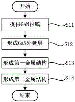
[0048] 在GaN基功率二极管制备方法的另一实施例中,如流程 Figure 9 shown, including the following steps:

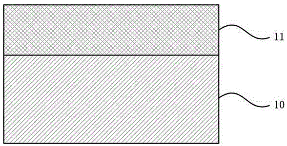
[0049] 步骤S21,提供GaN衬底20。优选为n型GaN衬底,掺杂浓度大于10 18 cm -3 .

[0050] 步骤S22,在GaN衬底20上形成GaN外延层21。例如,采用金属有机物化学气相淀积法(MOCVD)外延20µm厚的n型GaN漂移层, 掺杂浓度优选为2×10 16 cm -3 .

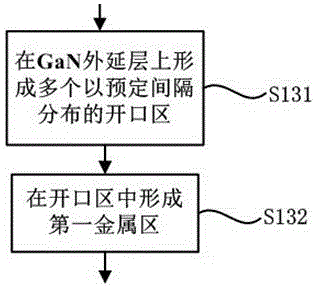
[0051] 步骤S23,形成第一金属层22并对其进行图形化,形成第一金属结构23,具体包括如下步骤:

[0052] 步骤S231,在GaN外延层21上形成第一金属外延层22,所得结构如 Figure 10 shown;

[0053] 步骤S232,对第一金属外延层22进行图形化,使部分所述GaN外延层暴露,形成多个以预定间隔分布的第一金属结构23,所得结构如 Figure 11 shown.

[0054] 步骤S24,在第一金属结构23上以及GaN外延层21上形成第二金属结构24,与GaN外延层21形成低势垒肖特基接触,所得结构如 Figure 12 shown. 具体地,例如,悬涂正性光刻胶,曝光出顶部电极区域。 然后,在器件顶部蒸镀0.5 µm厚度的与GaN外延层形成低势垒肖特基的金属,优选为Ti / Au,去胶后获得第二金属结构24。

[0055] 优选地,如流程 Figure 9 所示,还包括底部电极形成步骤S25,在步骤S21前执行步骤S25,即在GaN衬底20背面形成底部电极25,与GaN衬底形成欧姆接触。具体地,例如淀积蒸镀钛 / 金金属,快速热退火处理后形成欧姆接触,所得结构如 Figure 13 shown. It should be understood that Figure 9 中所示的具体步骤提供了根据本发明的实施方案的制备GaN基功率二极管的特定方法。 根据可替代的实施方案也可以执行其他顺序的步骤。 例如,本发明的可替代的实施方案可以以不次序执行以上所概括的步骤。 also, Figure 9 中所示的单独步骤可以包括可以以各种次序执行的多个子步骤,只要适合于单独步骤即可。此外,根据特定的应...


PUM

PropertyMeasurementUnit
thicknessaaaaaaaaaa

Abstract

The invention belongs to the technical field of semiconductor power electronic devices, and particularly discloses a GaN-based power diode and a preparation method thereof. The GaN-based power diode comprises a GaN substrate, a GaN epitaxial layer, first metal structures and a second metal structure, wherein the GaN substrate has first doping concentration; the GaN epitaxial layer is located on the GaN substrate and has second doping concentration; the second doping concentration is smaller than the first doping concentration; the first metal structures are distributed on the GaN epitaxial layer or in the GaN epitaxial layer at predetermined intervals; the second metal structure is formed on the first metal structures and the GaN epitaxial layer; the first metal structures and the GaN epitaxial layer form high barrier schottky contact; and the second metal structure and the GaN epitaxial layer form low barrier schottky contact. The GaN-based power diode has good reliability and relatively high reverse breakdown voltage when P-type doping on a GaN material is omitted.

Description

technical field [0001] The invention belongs to the technical field of semiconductor power electronic devices, and in particular relates to a GaN-based power diode and a preparation method thereof. Background technique [0002] With the rapid development of information technology, high-power electronic devices such as power switches and power rectifiers have been widely used in various fields of national economy. As a substitute for traditional silicon-based power devices, power devices based on the third-generation wide-bandgap semiconductor GaN materials have attracted much attention because of their excellent material properties and device structure. GaN materials have a large bandgap and electron mobility. Good thermal stability and chemical stability, so it has a wide application prospect in the field of high power and high frequency, and has attracted attention and research. Today, breakthroughs have been made in GaN-based high electron mobility transistors, but the r...

Claims


Application Information

Patent Timeline
Patent Type & Authority Applications(China)
IPC IPC(8): H01L29/861H01L29/06H01L21/329
CPCH01L29/872H01L29/0688H01L29/66143
Inventor 陈琳戴亚伟郑亮孙清清张卫
Owner FUDAN UNIV
Why Eureka
Try Eureka