Organic light emitting diode and manufacturing method thereof and display device

A technology for light-emitting diodes and a manufacturing method, which is applied in the manufacture of semiconductor/solid-state devices, electrical components, and electrical solid-state devices, etc., can solve the problems of difficult carrier balance and difficult material selection, etc.

Active Publication Date: 2016-08-24
BOE TECH GRP CO LTD
View PDF11 Cites 6 Cited by
  • Summary
  • Abstract
  • Description
  • Claims
  • Application Information

AI Technical Summary

Problems solved by technology

However, in this kind of light-emitting diode, it is difficult to choose materials, which makes it difficult to balance the carriers in the light-emitting process. Therefore, light-emitting diodes of a specific color are prone to emit light of other colors.

Method used


Image

  • Organic light emitting diode and manufacturing method thereof and display device
  • Organic light emitting diode and manufacturing method thereof and display device
  • Organic light emitting diode and manufacturing method thereof and display device

Examples


Embodiment 1

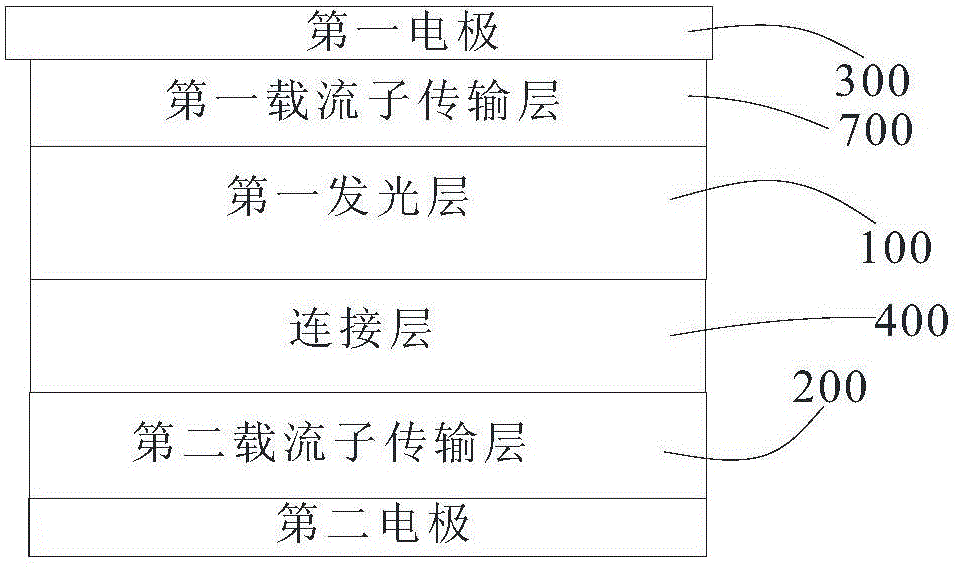
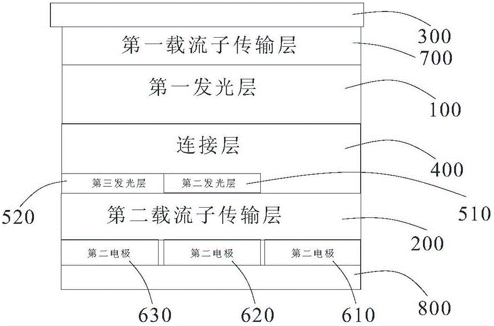
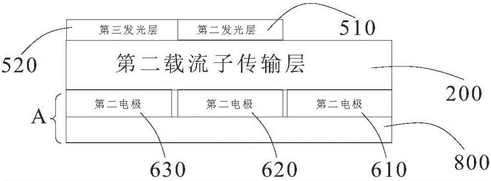
[0104] Organic Light Emitting Diodes have figure 2 In the structure, the first electrode 300 is a cathode, the first carrier transport layer 700 is an electron transport layer, the first light emitting layer 100 is a blue light emitting layer, the second light emitting layer 510 is a red light emitting layer, and the third light emitting layer 510 is a red light emitting layer. Layer 520 is a blue light-emitting layer, the second carrier transport layer 200 is a hole transport layer, the second electrode is an anode, and the thickness of the connection layer 400 is 1 nm.

Embodiment 2

[0106] The organic light emitting diode has the same structure as that of the organic light emitting diode in Embodiment 1, except that the connection layer 400 has a thickness of 5 nm.


PUM

PropertyMeasurementUnit
Thicknessaaaaaaaaaa
Thicknessaaaaaaaaaa
Thicknessaaaaaaaaaa

Abstract

The invention provides an organic light emitting diode. The organic light emitting diode comprises a first function part and a second function part which are arranged in a laminating manner; the first function part comprises a first carrier transporting layer and a first light emitting layer which are sequentially arranged in a laminating manner; the second function part comprises a second carrier transporting layer; the first function part and the second function part are produced by adopting different methods; the first function part also comprises a connecting layer; the connecting layer is positioned between the first light emitting layer and the second function part; the first light emitting layer comprises matrix materials and dopants doped in the matrix materials; the matrix materials comprise an N type matrix material and a P type matrix material. The organic light emitting diode provided by the invention has the effects of stably emitting light and obtaining light with ideal color.

Description

technical field [0001] The present invention relates to the field of display devices, and in particular, relates to an organic light emitting diode, a method for manufacturing the organic light emitting diode, and a display device including the organic light emitting diode. Background technique [0002] An organic light emitting diode includes an anode layer, a hole injection layer, a hole transport layer, a light emitting layer, an electron transport layer, an electron injection layer and a cathode which are stacked in sequence. At present, the above-mentioned different layers are usually formed by vacuum evaporation. [0003] Organic light-emitting diodes comprising multiple layers are generally produced using different processes. For example, a cathode layer, an electron injection layer, an electron transport layer, and a light emitting layer can be formed by vacuum evaporation, and a hole transport layer and a hole injection layer can be formed by a solution method. In...

Claims


Application Information

Patent Timeline
IPC IPC(8): H01L51/50H01L51/56H01L27/32
CPCH10K30/865H10K50/16H10K50/15H10K50/11H10K71/00H10K59/875H10K59/35H10K50/131H10K50/156H10K50/166H10K50/81H10K50/82H10K59/00H10K2101/10
Inventor 吴长晏尤娟娟宋莹莹闫光
Owner BOE TECH GRP CO LTD
Why Eureka
Try Eureka