A charge pump control circuit
A charge pump control and charge pump technology, applied in the field of circuits, can solve the problems of voltage fluctuation, difficult control and unsatisfactory effect of the charge pump circuit.
- Summary
- Abstract
- Description
- Claims
- Application Information
AI Technical Summary
Problems solved by technology
Method used
Image
Examples
Embodiment 1
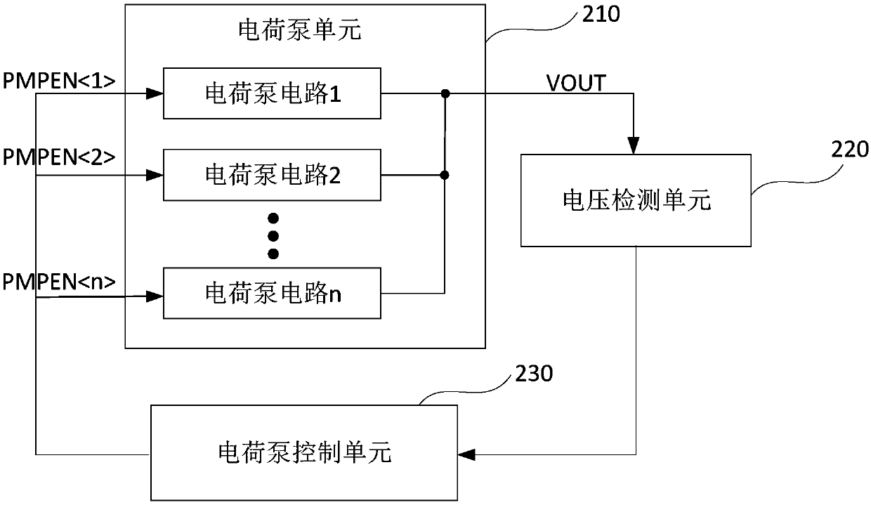
[0040] figure 2 It is a schematic structural diagram of a charge pump control circuit provided by Embodiment 1 of the present invention. This embodiment is applicable to the case where multiple charge pump circuits work in parallel in order to meet the readout time requirement of the Flash chip. Such as figure 2 As shown, a schematic structural diagram of a charge pump control circuit provided in this embodiment includes: a charge pump unit 210 , a voltage detection unit 220 and a charge pump control unit 230 .
[0041] The charge pump unit 210 includes at least two charge pump circuits, and the charge pump circuits are connected in parallel to each other for generating voltage; the input end of the voltage detection unit 220 is connected with the output end of the charge pump unit 210 for detecting the Whether the output voltage of the output terminal reaches the target voltage value, if so, then output the first flag signal to the charge pump control unit 230, otherwise o...
Embodiment 2
[0045] Figure 4 It is a schematic structural diagram of the voltage detection unit provided in Embodiment 2 of the present invention. On the basis of the above embodiments, this embodiment optimizes the voltage detection unit 220, see Figure 4 As shown, the voltage detection unit 220 includes: a voltage divider module 221 and a flag signal generation module 222, wherein the voltage divider module 221 is used to divide the voltage of the output terminal of the charge pump unit 210; The output terminal voltage of the pump unit 210 generates a first flag signal or a second flag signal.
[0046] Preferably, as an implementation of the voltage detection unit 220, see Figure 5 As shown, the voltage dividing module 221 includes: a first resistor R1, a second resistor R2 and a third resistor R3, and the flag signal generating module 222 includes a first comparator COMP1 and a second comparator COMP2, wherein:
[0047] The first terminal of the first resistor R1 is connected to th...
Embodiment 3
[0051] Figure 6 It is a schematic structural diagram of the charge pump control unit provided in Embodiment 3 of the present invention. On the basis of the above embodiments, this embodiment optimizes the charge pump control unit 230. Refer to Figure 6 As shown, the charge pump control unit 230 includes a ripple reduction circuit 231, a selection circuit 232, a control signal trigger circuit 233 and a charge pump enable signal generation circuit 234;
[0052] Wherein, the first input end of the ripple reduction circuit 231 is connected with the output end of the voltage detection unit 220, and the second input end is connected with the control signal trigger circuit 233, which is used to generate a control signal for controlling the working mode of the selection circuit 232; the selection circuit 232 The first input end of the voltage detection unit is connected to the output end of the voltage detection unit 220, the second input end is connected to the control signal trigg...
PUM
 Abstract
Description
Claims
Application Information


