Fan-out type wafer-level packaging method for semiconductor device
A wafer-level packaging and fan-out technology, applied in semiconductor devices, semiconductor/solid-state device manufacturing, electric solid-state devices, etc., can solve the difficulty of controlling the dimensional accuracy of rewiring layer thickness and width, and the difficulty of ensuring the flatness of the front of the chip , poor heat dissipation performance and other problems, to achieve the effect of ensuring flatness, improving heat dissipation performance, and improving precision
- Summary
- Abstract
- Description
- Claims
- Application Information
AI Technical Summary
Problems solved by technology
Method used
Image

Examples
Embodiment Construction
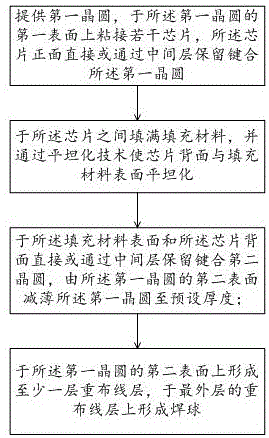
[0022] In order to solve the above-mentioned problems in the prior art, the present invention provides a fan-out wafer-level packaging method for semiconductor devices. The chip and the first wafer are bonded directly or through an intermediate layer to maintain a bonded state, without the need for In the subsequent process, the first wafer is separated and removed, so the pads on the front of the chip do not need to be opened before bonding, which can effectively ensure the flatness of the chip, improve the accuracy of the rewiring layer, and make the back of the chip and the filling material through the planarization technology Surface planarization reduces package height and improves heat dissipation.
[0023] In the following detailed description of the preferred embodiment, reference is made to the accompanying drawings which form a part hereof. The accompanying drawings show, by way of example, specific embodiments in which the invention can be practiced. The illustrate...
PUM
 Abstract
Description
Claims
Application Information
 - Generate Ideas
- Intellectual Property
- Life Sciences
- Materials
- Tech Scout
- Unparalleled Data Quality
- Higher Quality Content
- 60% Fewer Hallucinations
Browse by: Latest US Patents, China's latest patents, Technical Efficacy Thesaurus, Application Domain, Technology Topic, Popular Technical Reports.
© 2025 PatSnap. All rights reserved.Legal|Privacy policy|Modern Slavery Act Transparency Statement|Sitemap|About US| Contact US: help@patsnap.com