Real-time online test system for gamma ray radiation response of semiconductor device

A radiation response and online testing technology, applied in the field of real-time online testing systems, can solve the problems of inaccurate needle insertion, inability to apply bias voltage, and inability to automatically program the time point of pulse testing, to avoid radiation damage and degradation, and to achieve accurate and efficient film retrieval. , Improve test efficiency and test accuracy

Active Publication Date: 2016-09-28
XIAN JIAOTONG LIVERPOOL UNIV
View PDF6 Cites 7 Cited by
  • Summary
  • Abstract
  • Description
  • Claims
  • Application Information

AI Technical Summary

Problems solved by technology

[0007] The purpose of the present invention is to provide a real-time on-line test system for gamma-ray radiation response of semiconductor devices, to solve the problem that the gamma-ray radiation response test systems of semiconductor devices in the pr

Method used


Image

  • Real-time online test system for gamma ray radiation response of semiconductor device
  • Real-time online test system for gamma ray radiation response of semiconductor device
  • Real-time online test system for gamma ray radiation response of semiconductor device

Examples


Embodiment Construction

[0022] The above solution will be further described below in conjunction with specific embodiments. It should be understood that these examples are used to illustrate the present invention and not to limit the scope of the present invention. The implementation conditions adopted in the examples can be further adjusted according to the conditions of specific manufacturers, and the implementation conditions not indicated are usually conventional conditions.

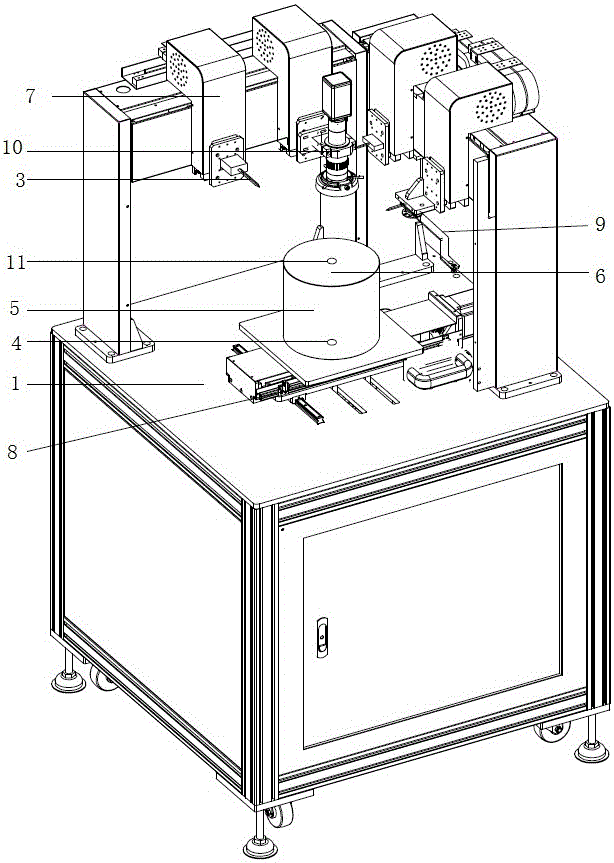
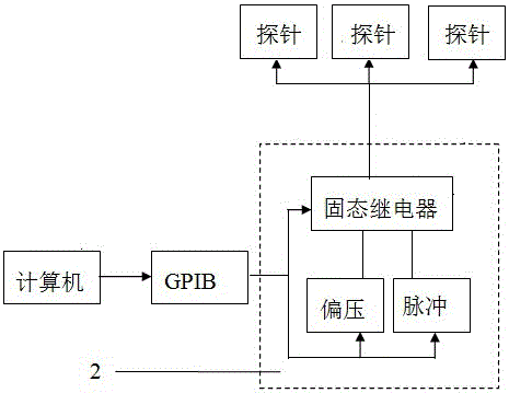
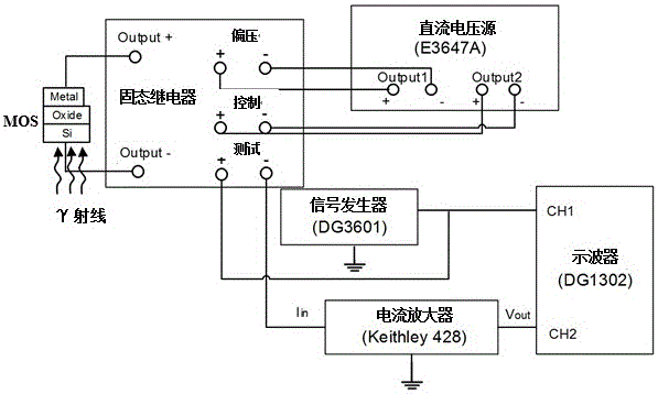
[0023] like figure 1 and 2 As shown, the real-time on-line test system of the gamma ray radiation response of the semiconductor device disclosed in the present invention includes a semiconductor device gamma ray test probe station 1 and a measurement module 2 that provides bias-pulse testing, on the test probe station 1 A lead container 5 with a built-in radioactive source 4, an automatic slicer 9, and four programmable probe arms 7 are installed, wherein a probe 3 is respectively installed on the three probe arms 7, and...


PUM


Abstract

The invention discloses a real-time online test system for gamma ray radiation response of a semiconductor device. The system comprises a semiconductor device gamma ray test probe station and a measuring module for providing bias-pulse test; a lead container in which a radiation source is arranged, an automatic taker and four programmable probe arms are installed on the test probe station, wherein one probe is separately installed on the three probe arms, a microscope is installed on the other probe arm, and the three probes are connected with the bias-pulse measuring module respectively. According to the system, high-precision remote sheet setting and needling are performed on the semiconductor device, then the radiation damage of the semiconductor device is tested on line via the programmable measuring module for providing bias-pulse test, bias can be simultaneously applied while the device to be tested is radiated, and the measured data is quickly stored. The system for sheet setting, needling and sheet taking is accurate and efficient, improves the test efficiency and the test precision, and avoids radiation damage and degradation caused by traditional radiation measurement means.

Description

technical field [0001] The invention relates to a real-time on-line test system for gamma ray radiation response of semiconductor devices. Background technique [0002] With the development of semiconductor materials, they are widely used in various industries. Among them, the electronic automation development of space technology, nuclear industry, nuclear power plants and radiation medical devices are all closely related to semiconductor materials. All kinds of applied electronic equipment in these industries are inevitably exposed to ionizing radiation, so the research on the radiation damage and radiation reliability of semiconductor devices in these electronic equipment in the radiation environment is very important. [0003] The traditional ionizing radiation reliability test of semiconductor materials uses radioactive sources or x-ray generators to irradiate semiconductor devices, and then conducts radiation damage measurement and analysis on another test platform, bu...

Claims


Application Information

Patent Timeline
IPC IPC(8): G01R31/26
CPCG01R31/2642
Inventor 慕轶非赵策洲
Owner XIAN JIAOTONG LIVERPOOL UNIV
Why Eureka
Try Eureka