A multi-active area light-emitting diode with p-i-n tunnel junction

A p-i-n, light-emitting diode technology, applied in electrical components, circuits, semiconductor devices, etc., can solve the problems affecting the performance of LEDs, affecting the quality of material crystals, etc., to achieve the effect of improving internal quantum efficiency, improving crystal quality, and increasing the probability of recombination

Active Publication Date: 2018-05-04
SOUTHEAST UNIV
View PDF7 Cites 0 Cited by
  • Summary
  • Abstract
  • Description
  • Claims
  • Application Information

AI Technical Summary

Problems solved by technology

[0005] The traditional pn tunnel junction uses heavy doping technology to obtain p + / n + However, in order to obtain a heavily doped p-type nitride layer, the nitride material must be heavily doped with metal Mg, and too high Mg doping will greatly affect the crystal quality of the material, thereby affecting the performance of the LED

Method used


Image

  • A multi-active area light-emitting diode with p-i-n tunnel junction
  • A multi-active area light-emitting diode with p-i-n tunnel junction
  • A multi-active area light-emitting diode with p-i-n tunnel junction

Examples


Embodiment

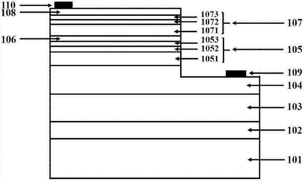
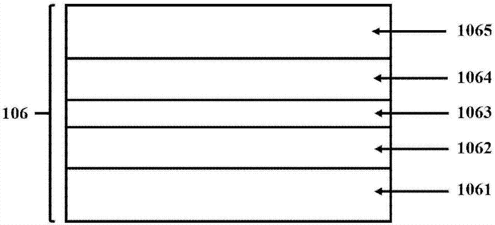
[0030] Such as figure 1 As shown, it is a multi-active-region LED with p-i-n tunnel junction provided by the present invention, which is characterized in that: from bottom to top, it includes a polar c-plane sapphire substrate 101, an AlN nucleation layer 102, an AlGaN buffer layer 103, and an n-type AlGaN layer 104, a first light emitting region 105, a p-i-n tunnel junction 106, a second light emitting region 107, and an indium tin oxide (ITO) conductive layer 108, wherein the light emitting region is made of Al x1 Ga 1-x1 N / Al x2 Ga 1-x2 N multiple quantum well active regions 1051 and 1071, p-type Al x3 Ga 1-x3 N electron blocking layers 1052 and 1072 and p-type AlGaN hole injection layers 1053 and 1073, where x 1 2 3 , lead out the n-electrode 109 and the p-electrode 110 on the n-region and the ITO conductive layer respectively. figure 2 A schematic diagram of the p-i-n tunnel junction layer structure of the multi-active area LED with p-i-n tunnel junction provided ...


PUM


Abstract

The invention discloses a multi-active region light emitting diode having a p-i-n tunnel junction. The diode includes, successively from the bottom to the top, a substrate, a nitride nucleation layer, a nitride buffer layer, an n-type nitride layer, a first light-emitting region, the p-i-n tunnel junction, a second light emitting region, and an indium tin oxide conductive layer. The first light emitting region consists of a first active region, a first p type nitride electronic barrier layer, and a first p type nitride cavity injection layer, and the second light emitting region consists of a second active region, a second p type nitride electronic barrier layer, and a second p type nitride cavity injection layer. According to the invention, the multi-active region light emission is realized, not only the electromigration problem brought by the electrode contact can be reduced, but also the width of the internal depletion region during the working of a traditional tunnel junction can be effectively reduced, and thereby the electronic tunneling distance is reduced, and the electronic tunneling probability is increased; and moreover, the crystal lattice mismatch caused by a traditional heavily doped tunnel junction can be effectively mitigated and the crystal quality of the device can be improved.

Description

technical field [0001] The invention provides a multi-active area light-emitting diode (LED) with p-i-n tunnel junction, which belongs to the field of manufacturing semiconductor optoelectronic materials and devices. Background technique [0002] As a new type of high-efficiency solid-state light source, LED has significant advantages such as energy saving, environmental protection, long life, small size, and low operating voltage. It has been widely used in lighting, display, environmental protection, communication and other fields. [0003] Such as image 3 , In existing LEDs based on III-V compound semiconductor materials, when a forward voltage is applied to the pn junction of the LED, a current will flow through the pn junction. The recombination of electrons and holes in the pn junction transition layer will generate photons. However, because the pn junction of the LED is a doped semiconductor, there are various defects in material quality, dislocation factors and proc...

Claims


Application Information

Patent Timeline
Patent Type & Authority Patents(China)
IPC IPC(8): H01L33/00
CPCH01L33/0012
Inventor 张雄王肖磊崔一平
Owner SOUTHEAST UNIV
Why Eureka
Try Eureka