Substrate processing apparatus and method of manufacturing semiconductor device
A substrate processing device and substrate technology, which are applied in semiconductor/solid-state device manufacturing, folders, electrical components, etc., can solve problems such as pattern size miniaturization
- Summary
- Abstract
- Description
- Claims
- Application Information
AI Technical Summary
Problems solved by technology
Method used
Image

Examples
no. 1 approach
[0035] Hereinafter, a first embodiment of the present invention will be described.
[0036]
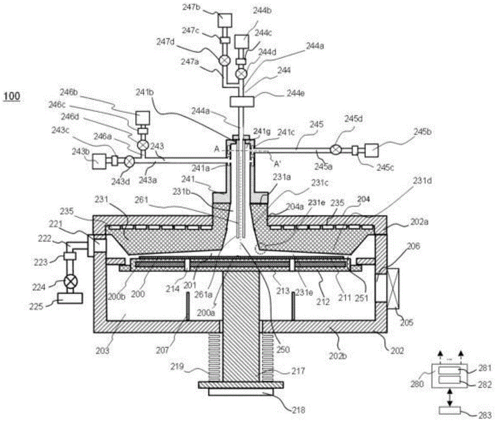
[0037] The structure of the substrate processing apparatus 100 of this embodiment is shown in figure 1 . Such as figure 1 As shown, the substrate processing apparatus 100 is configured as a monolithic substrate processing apparatus.
[0038] (processing container)
[0039] Such as figure 1 As shown, the substrate processing apparatus 100 includes a processing vessel 202 . The processing container 202 is configured, for example, as a closed container having a circular cross section and a flat shape. In addition, the processing container 202 is made of metal materials such as aluminum (Al) and stainless steel (SUS), for example. Formed in the processing container 202 are: a reaction zone 201 (reaction chamber) for processing a wafer 200 such as a silicon wafer as a substrate; The processing container 202 is composed of an upper container 202a and a lower container 202b.
[004...
no. 2 approach
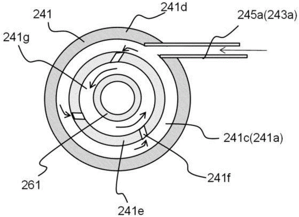
[0139] Next, use Figure 9 Next, a second embodiment will be described. Figure 9 It is an enlarged view of the tube front end 261a.
[0140] First, use Figure 12 A comparative example will be described. Arrow 301 indicates the flow of gas (gas containing the first element) outside the tube 261 , and arrow 302 indicates the flow of gas (gas containing the second element) supplied from the inside of the tube 261 .
[0141] Since the tip 303 is angular, the gas containing the first element supplied in the first processing gas supply step S202 collides with the outer peripheral tip 303 of the tube constituting the tube 261 and adheres thereto. Furthermore, since the tip 303 of the tube 261 is angular, the gas detoured to the tip 304 on the inner peripheral side of the tube 261 collides with and adheres thereto.
[0142] Therefore, when the gas containing the second element is supplied in the second gas supply step S206, the gas containing the second element contacts and reac...
Embodiment approach 3
[0145] Next, use Figure 10 Embodiment 3 will be described. In the present embodiment, the tip of the tube 261 is widened toward the treatment area 201 . With such a structure, since the gas containing the second element flows along the front end, it is easy to merge with the eddy flow flowing on the outer periphery of the tube 261 .
PUM
 Abstract
Description
Claims
Application Information