Manufacturing method and structure of trench gate power device

A technology of a power device and a manufacturing method, which is applied to the manufacture of trench gate power devices and the field of trench gate power devices, can solve problems such as reducing on-resistance, and achieve the effects of reducing on-resistance, good adjustment, and reducing cell size

Active Publication Date: 2019-08-13
SHANGHAI HUAHONG GRACE SEMICON MFG CORP
View PDF4 Cites 0 Cited by
  • Summary
  • Abstract
  • Description
  • Claims
  • Application Information

AI Technical Summary

Problems solved by technology

This limits the possibility of reducing the on-resistance by reducing the size of the platform between the trenches. The size of the platform between the trenches is also the distance between the trenches, that is, the width of the epitaxial layer between the trenches.

Method used


Image

  • Manufacturing method and structure of trench gate power device
  • Manufacturing method and structure of trench gate power device
  • Manufacturing method and structure of trench gate power device

Examples


Embodiment Construction

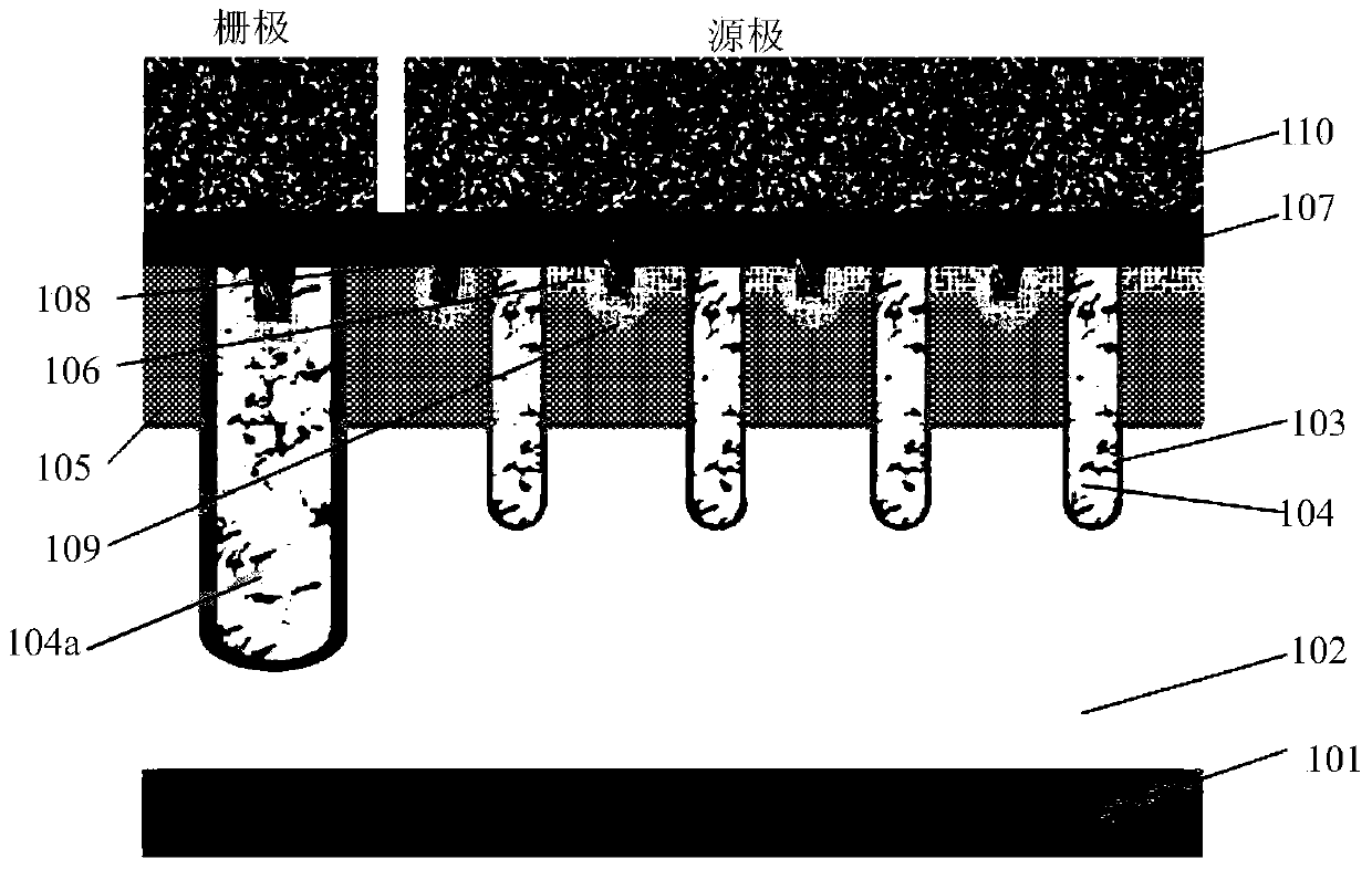
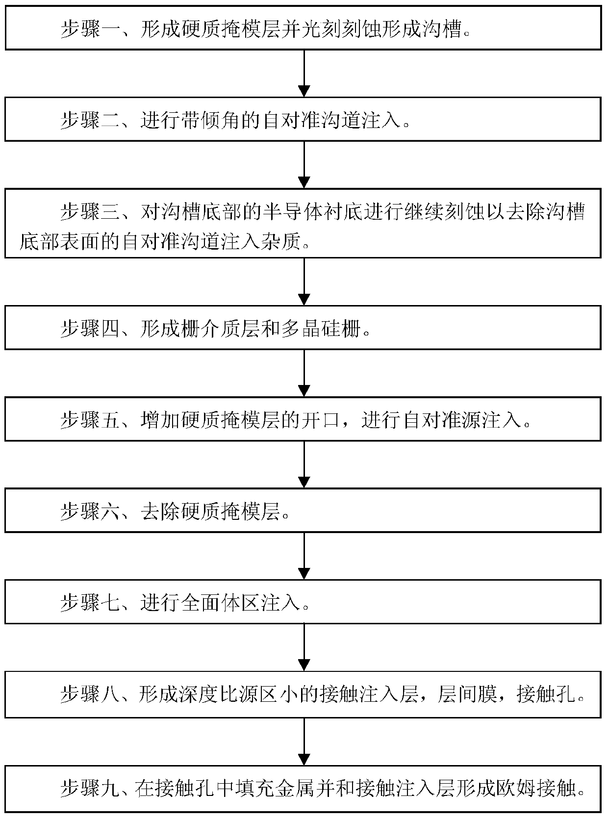
[0061] Such as figure 2 Shown is a flowchart of a method for manufacturing a trench gate power device according to an embodiment of the present invention; Figure 3A to Figure 3S Shown is the device structure diagram of each step of the manufacturing method of the trench gate power device in the embodiment of the present invention. In the manufacturing method of the trench gate power device in the embodiment of the present invention, the conduction region of the trench gate power device is composed of multiple original Cells are periodically arranged, and a gate electrode connection area is also included outside the conduction region of the trench gate power device; the forming steps of each cell in the conduction region of the trench gate power device include:

[0062] Step 1, such as Figure 3A As shown, a semiconductor substrate 1 is provided; preferably, the semiconductor substrate 1 is a silicon substrate and a semiconductor epitaxial layer 2 of a first conductivity typ...


PUM


Abstract

The invention discloses a trench gate power device manufacturing method, and the method comprises the steps: forming a hard mask layer, carrying out the photoetching and forming a trench; carrying out the self-aligning channel injection with an inclination angle; continuing the etching of a semiconductor substrate at the bottom of a trench, so as to remove the channel injection impurities on the surface of the bottom of the trench; forming a gate medium layer and a polysilicon gate; adding an opening of the hard mask layer, and carrying out the self-aligning source injection; removing the hard mask layer; carrying out the complete body region injection; forming a contact injection layer with the depth being less than the depth of a source region, and forming an interlayer film and a contact hole; carrying out the self-aligning contact injection formation after the contact injection layer is formed through complete contact injection before the interlayer film is formed or after the etching of the contact hole; placing metal in the contact hole, and forming ohmic contact with the contact injection layer. The invention also discloses a trench gate power device. The method can prevent the contact hole from passing through a source region, can improve the stability of a threshold voltage of the device, can reduce the size of a device unit, and can reduce the conduction resistance.

Description

technical field [0001] The invention relates to a manufacturing process method of a semiconductor integrated circuit, in particular to a manufacturing method of a trench gate power device. The invention also relates to a trench gate power device. Background technique [0002] In the existing manufacturing method of trench gate power devices, the conduction region of the device is composed of a plurality of cells, that is, unit structures (cells), such as forming a parallel structure. A contact hole needs to be cut through the source region to connect the body region at the bottom of the source region. In the actual process, the registration redundancy of the contact hole and the trench should be considered, and the gap between the contact hole and the trench should be large enough to prevent the threshold voltage drift caused by the offset of the contact hole exposure. This limits the possibility of reducing the on-resistance by reducing the size of the mesa between the tr...

Claims


Application Information

Patent Timeline
Patent Type & Authority Patents(China)
IPC IPC(8): H01L21/336H01L29/423H01L29/78
CPCH01L29/4236H01L29/66477H01L29/78
Inventor 柯行飞
Owner SHANGHAI HUAHONG GRACE SEMICON MFG CORP
Why Eureka
Try Eureka