Teflon fixture and its application for wet process of semiconductor micro-nano devices

A wet process, Teflon clip technology, applied in semiconductor/solid-state device manufacturing, electrical components, circuits, etc., can solve the problems of hindering ultraviolet light passing through, lithography failure, etc., to achieve the effect of convenient operation and portability

Inactive Publication Date: 2019-06-25
WUHAN UNIV OF TECH
View PDF5 Cites 0 Cited by
  • Summary
  • Abstract
  • Description
  • Claims
  • Application Information

AI Technical Summary

Problems solved by technology

Whether the lithography mask is clean is an important reason for the success of the lithography process. If there are pollutants on the mask, it will hinder the passage of ultraviolet rays and eventually lead to the failure of lithography.

Method used


Image

  • Teflon fixture and its application for wet process of semiconductor micro-nano devices
  • Teflon fixture and its application for wet process of semiconductor micro-nano devices

Examples


Embodiment Construction

[0049] The present invention will be further described below with reference to the accompanying drawings and embodiments.

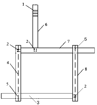
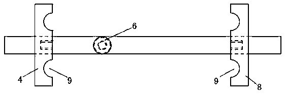
[0050] like figure 1 and figure 2 As shown, a kind of Teflon clamp for wet process of semiconductor micro-nano device includes a first clamping plate 4, a second clamping plate 8, a first sliding rod 7, a second sliding rod 3 and a handle 6, the first clamping plate 4 It is arranged in parallel with the second plywood 8, one end of the first sliding rod 7 is vertically fixed on the first plywood 4, the other end is matched with the second plywood 8, and one end of the second sliding rod 3 is vertically fixed on the second plywood 8 , the other end fits through the first clamp plate 4 (the first clamp plate 4 is provided with a through hole 5 that cooperates with the second slide bar 3, and the second clamp plate 8 is provided with a through hole 5 that cooperates with the first slide bar 7) , the handle 6 is fixed on the first sliding rod 7 (the handle...


PUM


Abstract

The invention relates to a teflon fixture for a wet process of a semiconductor micron / nano device and an application thereof. The teflon fixture comprises a first clamp plate, a second clamp plate, a first slide rod, a second slide rod and a handle, wherein the first clamp plate and the second clamp plate are disposed in parallel; one end of the first slide rod is perpendicularly fixed on the first clamp plate, and the other end of the first slide rod passes through the second clamp plate in a matched manner; one end of the second slide rod is perpendicularly fixed on the second clamp plate, and the other end of the second slide rod passes through the first clamp plate in a matched manner; the handle is fixed on the first slide rod or the second slide rod; and card slots which are matched with each other are respectively formed in surfaces, which are just opposite to each other, of the first clamp plate and the second clamp plate. The first clamp plate, the second clamp plate, the first slide rod, the second slide rod and the handle are all made from teflon materials. The fixture is simple in structure and convenient to clamp; the fixture can be applied to the wet process such as cleaning, etching, developing, rinsing, removing of photoresist and the like, of the semiconductor micron / nano device, and is high in efficiency and convenient to operate.

Description

technical field [0001] The invention belongs to the field of micro-processing technology of semiconductor micro-nano devices, in particular to a Teflon clamp used for wet process of semiconductor micro-nano devices and its application. Background technique [0002] At present, in the micromachining process of semiconductor devices, single crystal silicon, silicon carbide, substrates with oxide layers, glass substrates, ceramic substrates and photolithography masks, all external media in contact with the substrate may be contaminated with impurities on the substrate. source. This mainly includes the following aspects: pollution of the substrate during processing and molding, pollution during UV lithography, environmental pollution, pollution caused by water, pollution caused by reagents, pollution caused by industrial gases, pollution caused by the process itself , human pollution, etc. In the manufacture of semiconductor micro-nano devices, the substrate and mask must be s...

Claims


Application Information

Patent Timeline
Patent Type & Authority Patents(China)
IPC IPC(8): H01L21/687H01L21/02
CPCH01L21/02041H01L21/687
Inventor 何亮袁慧杨威麦立强
Owner WUHAN UNIV OF TECH
Why Eureka
Try Eureka