Accumulating type shield grid MOSFET integrating schottky diodes

A schottky diode, accumulation type technology, applied in the direction of electrical components, circuits, semiconductor devices, etc., can solve the problems of large leakage, complicated process steps, etc., achieve small on-resistance, reduce process steps, and reduce conduction voltage drop effect

Inactive Publication Date: 2016-10-12
UNIV OF ELECTRONICS SCI & TECH OF CHINA
View PDF6 Cites 7 Cited by
  • Summary
  • Abstract
  • Description
  • Claims
  • Application Information

AI Technical Summary

Problems solved by technology

[0005] The purpose of the present invention is to solve the problem that the Schottky diode has a large leakage when it is reverse-biased and the process steps are complicated. An accumulation-type shielded gate MOSFET with integrated Schottky diode is proposed. The process is relatively simple and easy to control. save chip area

Method used


Image

  • Accumulating type shield grid MOSFET integrating schottky diodes
  • Accumulating type shield grid MOSFET integrating schottky diodes
  • Accumulating type shield grid MOSFET integrating schottky diodes

Examples


Embodiment Construction

[0017] The present invention will be described in detail below in conjunction with the accompanying drawings.

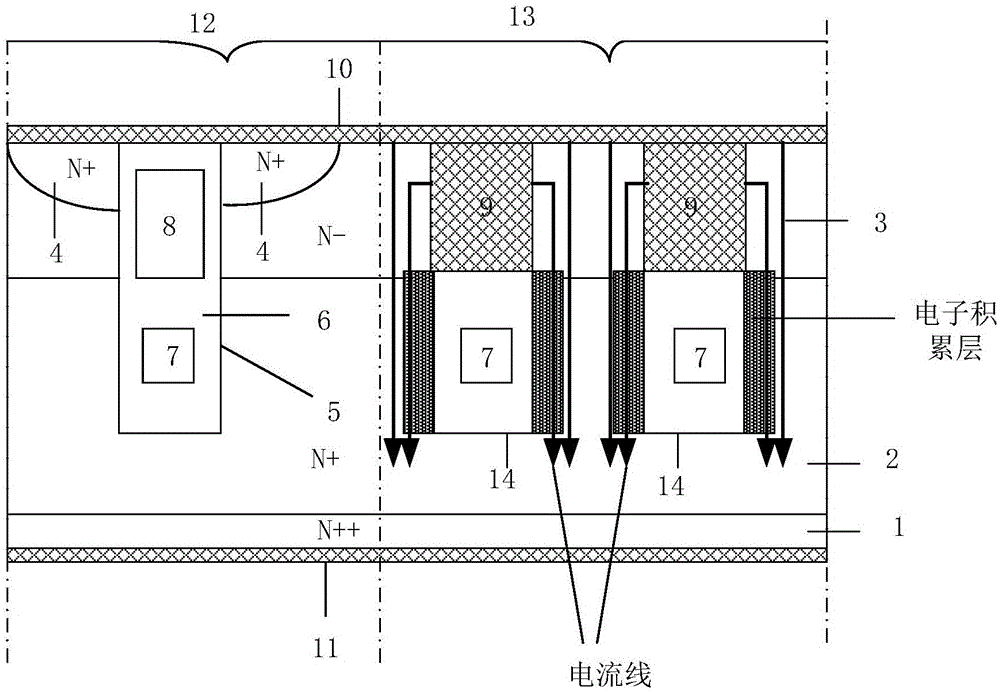
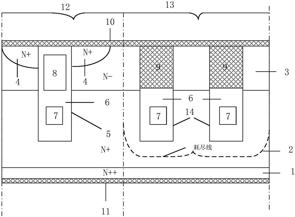
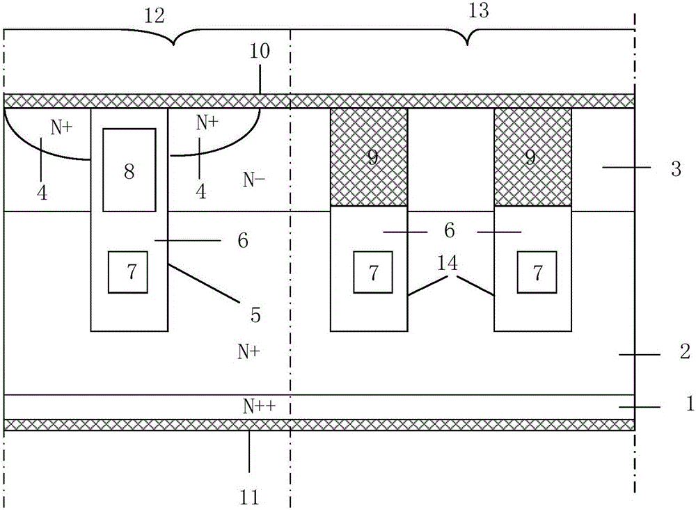
[0018] An accumulation-type shielded gate MOSFET integrating Schottky diodes according to the present invention, such as figure 1 As shown, it includes a MOSFET region 12 and a Schottky region 13; the MOSFET region 12 and the Schottky region 13 both include a first metal layer 11, an N++ type heavily doped substrate 1, an N+ type drift region 2, N-type doped region 3 and second metal layer 10; the N-type doped region 3 of the MOSFET region 12 has a first groove 5 and an N+ type heavily doped region 4; the N+ The upper surface of the type heavily doped region 4 is in contact with the second metal layer 10; the first groove 5 is located between the N+ type heavily doped region 4, and the lower end of the first groove 5 extends into the N+ type drift region 2; The upper surface of the first groove 5 is in contact with the second metal layer 10, the first groove 5 is f...


PUM


Abstract

The invention belongs to semiconductor technology, and specifically relates to an accumulating type shield grid MOSFET integrating a schottky diode. A shield grid MOSFET area formed on a silicon substrate is separated from and adjacent to a schottky diode forming area. The accumulating type shield grid MOSFET has a shield grid structure, and the schottky diode has a groove structure identical to that of the shield grid MOSFET, and the schottky diode is filled in the top of the groove through source electrode metal to form a schottky contact on the side surface of the groove to reduce a chip occupied area. The forming process of the schottky diode is compatible with the forming process of MOSFET, thereby reducing process steps. When the schottky diode is reversely biased, an electric field exists between a polysilicon 7 in the groove 14 and N+ drift region 2, the N+ drift region 2 generates depletion, and the depletion area extends to the N+ drift region 2 until complete depletion. The breakdown of schottky junctions is prevented, and reverse current leakage of schottky diode is minimized.

Description

technical field [0001] The invention belongs to the technical field of semiconductors, in particular to an accumulation-type shielded gate MOSFET integrated with Schottky diodes. Background technique [0002] Synchronous rectification in high-performance converter designs is critical for low-voltage, high-current applications because efficiency and power density can be significantly improved by replacing Schottky rectification with synchronous rectification MOSFETs. In practical applications, the power loss of synchronous rectification MOSFET is mainly composed of conduction loss, switching loss and body diode conduction loss. For example, in the power loss of the low-side power switch in the DC-DC conversion circuit, the conduction loss of the body diode still affects the overall loss of the MOSFET. With the increase of high frequency and high current requirements in power switching applications, the need to reduce power loss has received more and more attention. [0003]...

Claims


Application Information

Patent Timeline
Patent Type & Authority Applications(China)
IPC IPC(8): H01L29/78H01L29/872H01L29/423H01L29/06
CPCH01L29/0611H01L29/0684H01L29/42356H01L29/7827H01L29/872H01L29/7806H01L29/7813H01L29/407
Inventor 李泽宏李爽陈文梅陈哲曹晓峰李家驹罗蕾任敏
Owner UNIV OF ELECTRONICS SCI & TECH OF CHINA
Why Eureka
Try Eureka