Switch capacitor integrator circuit for eliminating offset voltage

A technology of offset voltage and switched capacitors, which is applied in the direction of voltage/temperature change compensation, reliability improvement and modification, etc. It can solve the problems that the final parameters cannot be matched, and the offset voltage of the amplifier is not considered, so as to achieve simple structure, high precision and wide application foreground effect

Active Publication Date: 2016-10-12
SHANGHAI ADVANCED RES INST CHINESE ACADEMY OF SCI
View PDF5 Cites 8 Cited by
  • Summary
  • Abstract
  • Description
  • Claims
  • Application Information

AI Technical Summary

Problems solved by technology

The traditional switched capacitor integrator circuit does not take into account the offset voltage of the amplifier, and the final parameters of the amplifier durin

Method used


Image

  • Switch capacitor integrator circuit for eliminating offset voltage
  • Switch capacitor integrator circuit for eliminating offset voltage
  • Switch capacitor integrator circuit for eliminating offset voltage

Examples


Embodiment 1

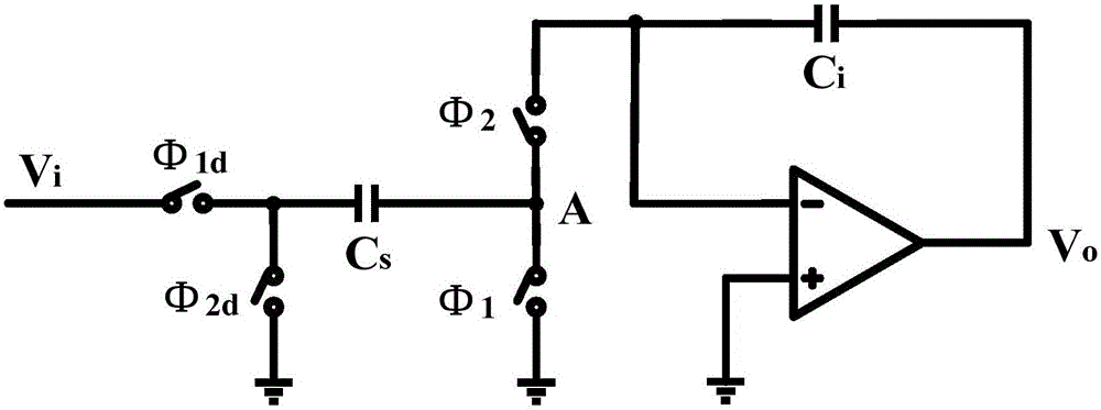
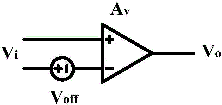
[0054] figure 1 Shown as a traditional switched capacitor integrator circuit, the traditional switched capacitor integrator circuit shown does not take into account the offset voltage present in the amplifier. During the manufacturing process of the amplifier, its final parameters cannot be completely matched with the design situation, so that the output voltage is not equal to the input voltage multiplied by the gain. In order to facilitate the analysis, an offset voltage V is generally superimposed on the input of the amplifier. off to simulate such non-ideal factors, such as figure 2 shown. At this time, the relationship between the output and input of the amplifier is equivalent to:

[0055] V o =A v (V i +V off )

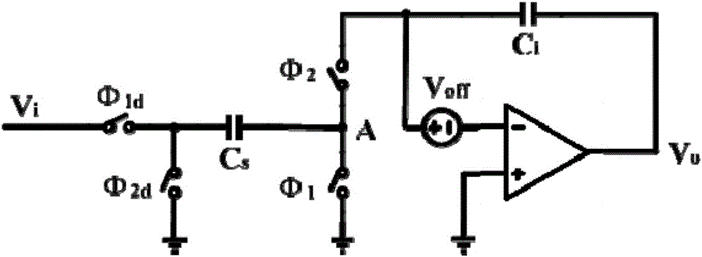
[0056] Among them, A v is the gain factor of the amplifier, when considering the offset voltage of the amplifier, the output value of the switched capacitor integrator is also affected by the offset voltage. image 3 is the switched capacitor integra...

Embodiment 2

[0078] Such as Figure 5 ~ Figure 7 As shown, this embodiment provides a switched capacitor integrator circuit for eliminating offset voltage.

[0079] In the analysis of embodiment 1, it is mentioned that some special occasions will use the inverter as the amplifier, and its structure is as follows Figure 5 shown. In a digital circuit, the input and output of the inverter are either 0 or 1, and its actual voltage value can only be close to the power supply voltage or ground. In this case, the inverter does not have an amplification function. In general, an inverter as an amplifier needs to bias its input and output bias voltages near half the power supply voltage in order to achieve a more ideal amplification effect. But because of this, an inverter cannot zero the voltage at its input through a "virtual ground" like a normal amplifier. exist Figure 5 In , the inverter will form a stable DC bias state through the feedback network, and at this time there will be a bias ...


PUM


Abstract

The invention provides a switch capacitor integrator circuit for eliminating offset voltage. The switch capacitor integrator circuit for eliminating the offset voltage comprises a first capacitor, a second capacitor, a third capacitor, a fourth capacitor, a first switch, a second switch, a third switch, a fourth switch, a fifth switch, an offset voltage source and an amplifier or a phase inverter. The size of integral output voltage of an amplifier offset voltage eliminating circuit of a switch capacitor integrator is unrelated to threshold voltage of the amplifier, and the precision of the integrator is improved; additionally, the offset voltage eliminating structure can be used for compensating integral offset caused by offset voltage inputted by the phase inverter when the phase inverter is taken as the amplifier. The switch capacitor integrator circuit for eliminating the offset voltage has a simple structure, and has the wide application prospect in the switch capacitor integrator circuit.

Description

technical field [0001] The invention relates to a switched capacitor integrator circuit, in particular to a switched capacitor integrator circuit for eliminating offset voltage. Background technique [0002] Modern integrated circuit design and signal processing are closely related to CMOS technology. However, the absolute value of resistors and capacitors in the CMOS process will fluctuate greatly during the manufacturing process, so that the direct use of resistors and capacitors in occasions with high precision requirements cannot meet the processing requirements for continuous signals. Among them, the continuous integrator uses this method to continuously integrate the analog signal. The advantage is that it has good real-time performance and does not require complicated timing control, such as non-overlapping clocks. [0003] It can be clearly seen that the continuous integrator will greatly reduce the integration accuracy due to the absolute error of the resistance an...

Claims


Application Information

Patent Timeline
IPC IPC(8): H03K19/003
CPCH03K19/00369
Inventor 汪辉叶汇贤田犁汪宁章琦曹虎黄景林
Owner SHANGHAI ADVANCED RES INST CHINESE ACADEMY OF SCI
Why Eureka
Try Eureka