Bicmos integrated circuit manufacturing method

A production method and integrated circuit technology, applied in the manufacture of circuits, electrical components, semiconductors/solid-state devices, etc., can solve problems such as the decline in product qualification rate, and achieve the effect of improving the qualification rate

Active Publication Date: 2019-04-02
FOUNDER MICROELECTRONICS INT
View PDF8 Cites 0 Cited by
  • Summary
  • Abstract
  • Description
  • Claims
  • Application Information

AI Technical Summary

Problems solved by technology

[0005] The invention provides a BiCMOS integrated circuit manufacturing method to solve the problem that the product qualification rate decreases due to the presence of water molecules on the surface of the thin oxide layer in the prior art

Method used


Image

  • Bicmos integrated circuit manufacturing method
  • Bicmos integrated circuit manufacturing method
  • Bicmos integrated circuit manufacturing method

Examples


Embodiment 1

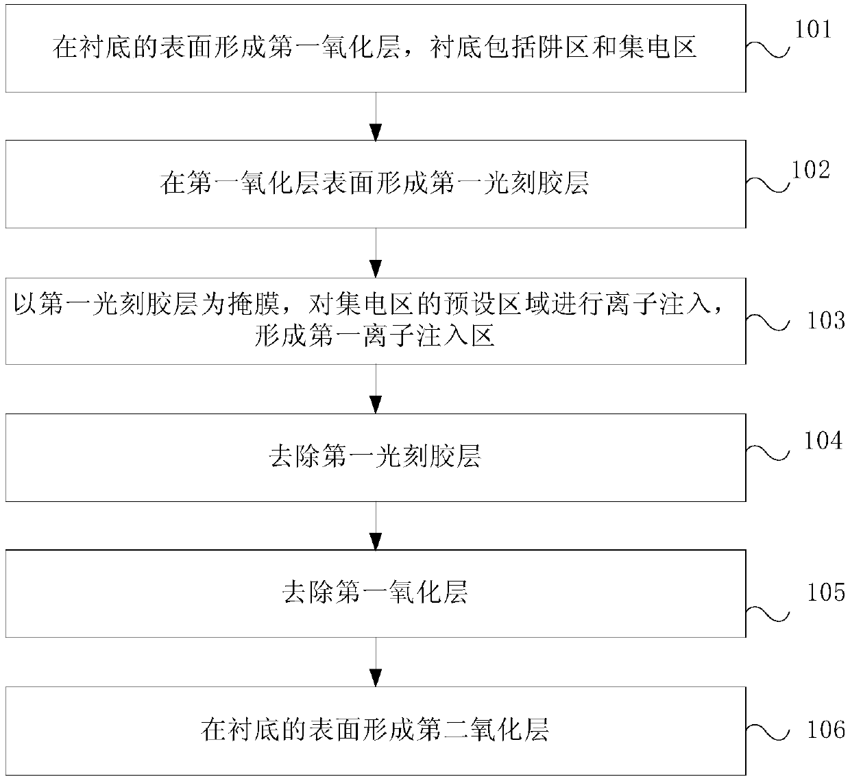
[0017] This embodiment provides a method for manufacturing a BiCMOS integrated circuit, which is used for manufacturing a BiCMOS integrated circuit. like figure 1 Shown is a schematic flow chart of the method for manufacturing a BiCMOS integrated circuit according to this embodiment.

[0018] In step 101, a first oxide layer is formed on the surface of the substrate, and the substrate includes a well region and a collector region.

[0019] The substrate in this embodiment may specifically be a silicon substrate, and the well region and the collector region may be arranged adjacent to each other. The first oxide layer is relatively thin, with a thickness ranging from 50 angstroms to 500 angstroms.

[0020] Step 102, forming a first photoresist layer on the surface of the first oxide layer.

[0021] A photoresist can be coated on the surface of the first oxide layer, and exposure, development and other processes are performed to remove the photoresist in the preset area and r...

Embodiment 2

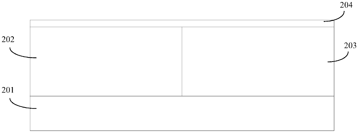
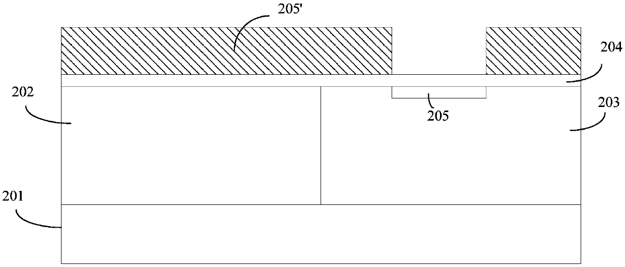
[0037] like Figure 2A to Figure 2K Shown is a structural schematic view of each step in the above-mentioned BiCMOS integrated circuit manufacturing method.

[0038] like Figure 2A Shown is a schematic structural view of a substrate 201 , and the substrate 201 includes a well region 202 and a collector region 203 .

[0039] The substrate 201 in this embodiment may be a P-type substrate, the collector region 203 is N-type, and the well region is P-type.

[0040] A first oxide layer 204 is formed on the surface of the substrate 201 .

[0041] Specifically, a thermal oxidation process may be used to form the first oxide layer 204 on the surface of the substrate 201 . The thickness of the first oxide layer 204 is 50 Å-500 Å. The material of the first oxide layer may be silicon oxide.

[0042] like Figure 2B As shown, a photoresist is coated on the surface of the first oxide layer 204, and processes such as exposure and development are performed on the photoresist to form t...


PUM


Abstract

The invention provides a BiCMOS integration circuit manufacturing method. The method comprises the following steps of forming a first oxide layer on a substrate surface, wherein a substrate includes a well region and a collecting area; forming a first photoresist layer on a first oxide layer surface; taking the first photoresist layer as a mask film, and carrying out ion implantation on a preset area of the collecting area so as to form a first ion implantation area; removing the first photoresist layer; removing the first oxide layer; and forming a second oxide layer on the substrate surface. By using the BiCMOS integration circuit manufacturing method of the invention, a qualified rate of a BiCMOS integration circuit can be increased.

Description

technical field [0001] The invention relates to semiconductor technology, in particular to a BiCMOS integrated circuit manufacturing method. Background technique [0002] BiCMOS (Bipolar Complementary Metal Oxide Semiconductor, bipolar gate circuit and complementary metal oxide semiconductor) integrated circuit is the integration of bipolar transistors (Bipolar) and complementary metal oxide semiconductor (Complementary Metal Oxide Semiconductor, CMOS) in the same chip The integrated circuit utilizes the advantages of Bipolar and CMOS and overcomes their shortcomings. Therefore, it not only has the advantages of high integration and low power consumption of CMOS, but also has the advantages of high-speed and high-current drive capabilities of bipolar devices. BiCMOS is a new generation of high-performance large-scale integrated circuits after CMOS. Among them, a bipolar transistor (Bipolar) is composed of an emitter region, a base region and a collector region, and a comple...

Claims


Application Information

Patent Timeline
Patent Type & Authority Patents(China)
IPC IPC(8): H01L21/782
Inventor 潘光燃文燕高振杰马万里石金成蔡新春
Owner FOUNDER MICROELECTRONICS INT
Why Eureka
Try Eureka