Pixel array and manufacturing method of display device comprising the pixel array

A technology for pixel arrays and display devices, which is applied in the manufacturing of semiconductor/solid-state devices, electric solid-state devices, semiconductor devices, etc., can solve the problems of small aperture size of masks, reduced product yield, increased process costs, etc. Process difficulty, reducing process cost and improving yield

Active Publication Date: 2016-10-19
EVERDISPLAY OPTRONICS (SHANGHAI) CO LTD
View PDF3 Cites 12 Cited by
  • Summary
  • Abstract
  • Description
  • Claims
  • Application Information

AI Technical Summary

Problems solved by technology

[0003] The pixel arrangement in the current OLED display device is generally a Pentile arrangement or an RGB arrangement, and when a mask is used to prepare a display device, the evaporated mask is used to define the pixel array located in the display area. A sub-pixel corresponds to a mask opening, and with the reduction of the size of the sub-pixel, the size of the mask opening becomes smaller and smaller, resulting in an increasingly accurate alignment when forming a pixel array by evaporation. High, the corresponding difficulty of the process is also increasing, which greatly reduces the yield of the product and increases the cost of the process

Method used


Image

  • Pixel array and manufacturing method of display device comprising the pixel array
  • Pixel array and manufacturing method of display device comprising the pixel array
  • Pixel array and manufacturing method of display device comprising the pixel array

Examples


Embodiment 1

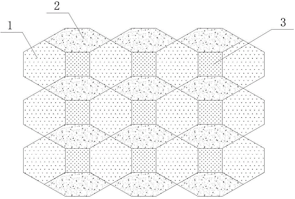
[0060] image 3 It is a schematic structural diagram of the pixel array in Embodiment 1 of the present invention; based on the above Figure 1~2 On the basis of the structure shown, in the first embodiment, each pixel unit includes two identical (identical in shape, length, area, material, etc.) sub-pixels, that is, the first pixel unit 1 includes the first For the sub-pixels 11 and 12 , the second sub-pixel unit 2 includes the second sub-pixels 21 and 22 , and the third sub-pixel unit 3 includes the third sub-pixels 31 and 32 .

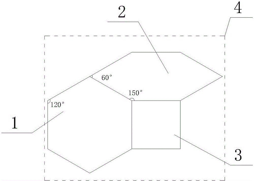
[0061] Figure 4 for image 3 Schematic diagram of the structure of a pixel unit in the image 3 In order to display clearly, the filling color in each pixel unit graph is also removed, that is, the same icon indicates the same device structure; as Figure 4 As shown, in the above-mentioned third pixel unit 3, on the midpoint of the side adjacent to the second pixel unit, a third median line perpendicular to the side is set (ie Figure 4 shown i...

Embodiment 2

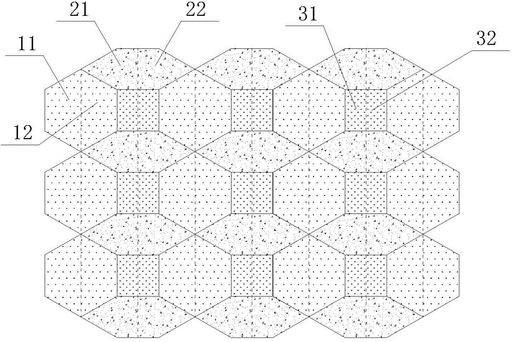
[0063] Figure 5 It is a schematic structural diagram of the pixel array in Embodiment 2 of the present invention; Image 6 for Figure 5 Schematic diagram of the structure of a pixel unit in the Image 6 In order to display clearly, the filling color in each pixel unit graph is also removed, that is, the same icon indicates the same device structure; as Figure 5-6 shown, based on the above Figure 1~4 On the basis of the structure shown and the relevant descriptions of Embodiment 1, in Embodiment 2, like Embodiment 1, each pixel unit also includes two identical (shape, length, area, material, etc.) ) sub-pixels, correspondingly the resolutions of the display devices formed by them are the same, that is, different pixel array structures are used to form the display devices with the same resolution.

[0064] Further, such as Image 6 As shown, compared with Embodiment 1 in Embodiment 2, in the second sub-pixel unit 2, diagonals with an angle of 60° are connected to form a...

Embodiment 3

[0066] Figure 7 It is a schematic structural diagram of the pixel array in Embodiment 3 of the present invention; Figure 8 for Figure 7 Schematic diagram of the structure of a pixel unit in the Figure 8 In order to display clearly, the filling color in each pixel unit graph is also removed, that is, the same icon indicates the same device structure; as Figure 7-8 shown, based on the above Figure 1~6 On the basis of the structure shown, the relevant descriptions of Embodiment 1 and Embodiment 2, each sub-pixel unit is divided into four sub-pixels, so that each sub-pixel can form a pixel that emits white light with sub-pixels of other light-emitting colors; Specifically, in the third embodiment, each pixel unit is composed of four sub-pixels, that is, the first sub-pixel unit includes the first sub-pixels 11, 12, 13, 14, and the second sub-pixel unit includes the second sub-pixel 21 , 22, 23, 24, the third sub-pixel unit includes third sub-pixels 31, 32, 33, 34.

[00...


PUM


Abstract

The invention provides a pixel array and a manufacturing method of a display device comprising the pixel array. Based on a traditional pixel array arrangement mode, sub-pixels with the same luminescence color are integrated into one sub-pixel unit. Based on the condition that pixel array luminescence is not influenced, a mask layer plate opening is used to form one sub-pixel unit in a manufacturing technology. Mask layer plate manufacturing difficulty is effectively reduced and simultaneously a precision requirement in a pixel array manufacturing technology can be greatly decreased. And the formed display device can satisfy a resolution requirement. Through one mask layer plate opening, a plurality of adjacent sub-pixels are formed. Technology difficulty can be effectively reduced, a yield rate of the device is increased and technology cost is reduced.

Description

technical field [0001] The invention relates to the field of manufacturing semiconductor devices, in particular to a pixel array and a method for manufacturing a display device including the pixel array. Background technique [0002] With the advancement of science and technology and the development of society, people have higher and higher requirements for the definition of display devices, which in turn makes the resolution of digital display devices higher and higher, and the size of sub-pixels in corresponding display devices is also getting higher and higher. come smaller. [0003] The pixel arrangement in the current OLED display device is generally a Pentile arrangement or an RGB arrangement, and when a mask is used to prepare a display device, the evaporated mask is used to define the pixel array located in the display area. A sub-pixel corresponds to a mask opening, and with the reduction of the size of the sub-pixel, the size of the mask opening becomes smaller an...

Claims


Application Information

Patent Timeline
Patent Type & Authority Applications(China)
IPC IPC(8): H01L27/32H01L51/56
CPCH10K59/122H10K71/00
Inventor 张斌林信志邹忠哲
Owner EVERDISPLAY OPTRONICS (SHANGHAI) CO LTD
Why Eureka
Try Eureka