A kind of impurity removal method for semi-melted ingot of polycrystalline silicon

A polysilicon ingot furnace and polysilicon technology, applied in polycrystalline material growth, chemical instruments and methods, single crystal growth, etc., can solve problems such as large fluctuation range, ineffective removal of impurities and oxygen, and impact on product quality , to achieve the effect of low input cost, convenient realization and easy mastery

Inactive Publication Date: 2018-10-12
XIAN HUAJING ELECTRONICS TECH
View PDF4 Cites 0 Cited by
  • Summary
  • Abstract
  • Description
  • Claims
  • Application Information

AI Technical Summary

Problems solved by technology

At present, the semi-melted ingot casting process of solar polysilicon ingots has been unanimously promoted by the market due to its advantages such as good crystal flowers. However, in the semi-melted ingot casting process, the impurities and oxygen in the raw materials have not been effectively melted because the silicon material on the side of the crucible has not been melted. The impurity removal will cause these impurities to form hard spots in the ingot casting process, which will have a great impact on the quality of the product
The existing semi-melted ingot casting process can control the hard point of the finished ingot at 3% to 5%, with a large fluctuation range, and this data is the data of the rough square flaw detection, the quasi-square data is higher and hard The point ratio is more than 5%

Method used


Image

  • A kind of impurity removal method for semi-melted ingot of polycrystalline silicon
  • A kind of impurity removal method for semi-melted ingot of polycrystalline silicon
  • A kind of impurity removal method for semi-melted ingot of polycrystalline silicon

Examples


Embodiment 1

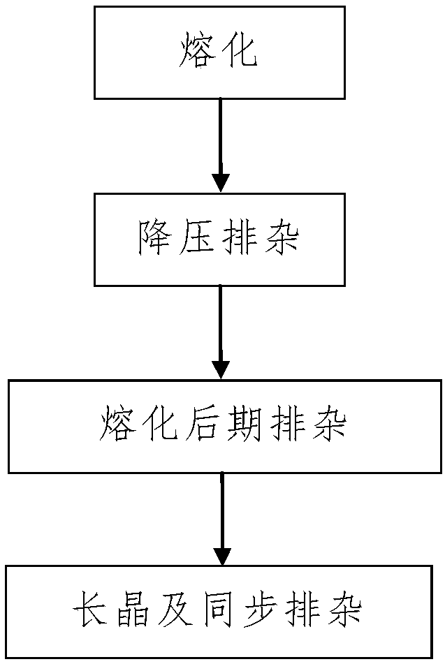
[0056] Such as figure 1 A kind of polysilicon semi-melting ingot shown is used for the impurity removal method, comprises the following steps:

[0057] Step 1, melting and removing impurities, the process is as follows:

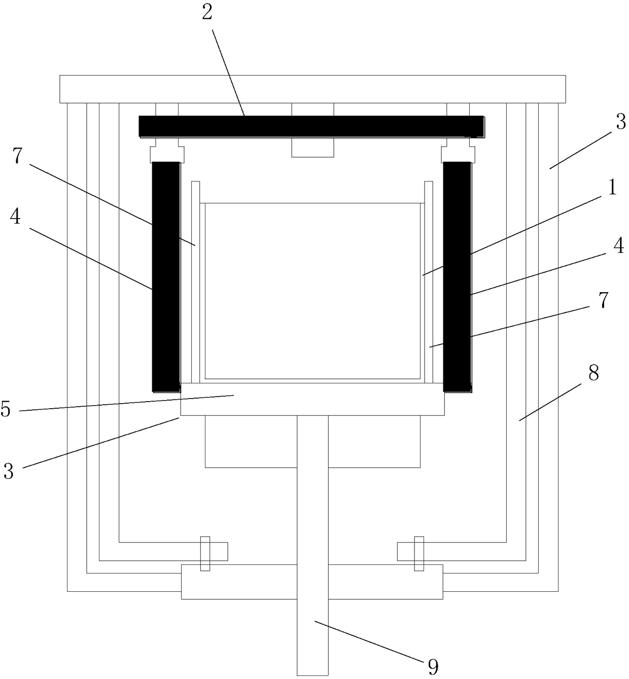
[0058] Step 101, Melting: After turning on the top heater 2 located above the crucible 1 in the polysilicon ingot furnace 3 and the four side heaters 4 respectively arranged on the outside of the four side walls of the crucible 1, according to the conventional polysilicon semiconductor The ingot melting method uses a polycrystalline silicon ingot furnace 3 to melt the silicon material contained in the crucible 1, and the melting temperature is T1 to T2; wherein, T1=1200°C, T2=1540°C;

[0059] During the melting process in step 101, inert gas is filled into the polysilicon ingot furnace 3 and the air pressure in the polysilicon ingot furnace 3 is kept at Q1, wherein Q1=600mbar;

[0060] Step 102, step down and remove impurities, the process is as follows:

...

Embodiment 2

[0114] In this embodiment, the difference from Embodiment 1 is that the P described in step 1 dmax 150kW, P cmax =220kW; T1=1125 DEG C in step 101, T2=1530 DEG C, heat preservation 8h when carrying out the first heat preservation in step 1012, heat preservation 14h when carrying out the second heat preservation in step 1013; Q2=350mbar in the step 1021, step-down time It is 12min, and the holding time in step 1022 is 60min; The time for continuing to melt in step 103 is 40min, T3=1420°C; T4=1410°C in step 2, and c in step 201 1 =0.9, c 0 =0.6, the crystal growth time in the early stage is 15h; in step 202 T5=1405°C, the crystal growth time in the later stage is 35h; the crystal growth rate in step 2 is controlled at 10mm / h; Q1 in step 1 and step 2=550mbar.

[0115] In this embodiment, the remaining method steps and process parameters are the same as those in Embodiment 1.

[0116] In this embodiment, the surface of the processed polysilicon ingot has no impurities, no sticky ...

Embodiment 3

[0118] In this embodiment, the difference from Embodiment 1 is that the P described in step 1 dmax 180kW, P cmax =260kW; T1=1285 DEG C in step 101, T2=1550 DEG C, heat preservation 4h when carrying out the first time heat preservation in step 1012, heat preservation 10h when carrying out the second heat preservation in step 1013; Q2=450mbar in the step 1021, step-down time It is 8min, and the holding time in step 1022 is 10min; the time for continuing to melt in step 103 is 15min, T3=1440°C; T4=1430°C in step 2, c in step 201 1 =0.8,c 0 =0.3, the crystal growth time in the early stage is 10h; in step 202 T5=1425°C, the crystal growth time in the later stage is 28h; the crystal growth rate in step 2 is controlled at 13mm / h; Q1 in step 1 and step 2=650mbar.

[0119] In this embodiment, the remaining method steps and process parameters are the same as those in Embodiment 1.

[0120] In this embodiment, the surface of the processed polysilicon ingot has no impurities, no sticky...


PUM

PropertyMeasurementUnit
thicknessaaaaaaaaaa

Abstract

The invention discloses a polycrystalline silicon semi-casting ingot impurity removing method, which comprises: 1, melting and impurity removing, wherein the process comprises: 101, melting: melting a silicon material loaded in a crucible by using a polycrystalline silicon ingot casting furnace, and introducing an inert gas into the polycrystalline silicon ingot casting furnace to carry out pressure maintaining, 102, pressure reducing impurity removing, and 103, impurity removing at late melting stage: increasing the pressure of the polycrystalline silicon ingot casting furnace, continuously melting the silicon material, and adjusting the heating powers of a top portion heater and / or four side portion heaters to make the top side ratio coefficient c of the polycrystalline silicon ingot casting furnace be more than or equal to 0.8 and less than 1; and 2, crystal growing and synchronous impurity removing, wherein the heating powers of the top portion heater and / or the four side portion heaters are adjusted to make the top side ratio coefficient c of the polycrystalline silicon ingot casting furnace be more than or equal to 0.3 and less than 0.9. According to the present invention, the method has characteristics of simple steps, reasonable design, convenient achieving, and good use effect; and with the synchronous impurity removing at the late material melting stage, the pressure reducing impurity removing and the crystal growing and synchronous impurity removing, the hard points of the casting finished product are effectively reduced, and the quality of the casting finished product can be effectively increased.

Description

technical field [0001] The invention belongs to the technical field of polycrystalline silicon ingots, and in particular relates to a method for removing impurities for semi-melted polycrystalline silicon ingots. Background technique [0002] Photovoltaic power generation is one of the most important clean energy sources with great development potential. The key factors restricting the development of photovoltaic industry are low photoelectric conversion efficiency on the one hand and high cost on the other hand. Photovoltaic silicon wafers are the basic material for the production of solar cells and components. The purity of polysilicon used to produce photovoltaic silicon wafers must be above 6N (that is, the total content of non-silicon impurities is below 1ppm), otherwise the performance of photovoltaic cells will be greatly negative influences. In recent years, the production technology of polycrystalline silicon wafers has made remarkable progress, and the polycrysta...

Claims


Application Information

Patent Timeline
Patent Type & Authority Patents(China)
IPC IPC(8): C30B28/06C30B29/06
CPCC30B28/06C30B29/06
Inventor 刘波波贺鹏蔺文虢虎平
Owner XIAN HUAJING ELECTRONICS TECH
Why Eureka
Try Eureka