Plasma enhanced chemical vapor deposition of films for improved vertical etch performance in 3D NAND memory devices

A plasma and film technology, applied in gaseous chemical plating, electrical components, electrical solid devices, etc., can solve problems such as plasma damage

Inactive Publication Date: 2016-10-26
APPLIED MATERIALS INC
View PDF0 Cites 16 Cited by
  • Summary
  • Abstract
  • Description
  • Claims
  • Application Information

AI Technical Summary

Problems solved by technology

However, the high energy required to achieve a straight etch profile using conventional single-operation etch recipes can result in plasma damage to the top surface of the structure

Method used


Image

  • Plasma enhanced chemical vapor deposition of films for improved vertical etch performance in 3D NAND memory devices
  • Plasma enhanced chemical vapor deposition of films for improved vertical etch performance in 3D NAND memory devices
  • Plasma enhanced chemical vapor deposition of films for improved vertical etch performance in 3D NAND memory devices

Examples


Embodiment Construction

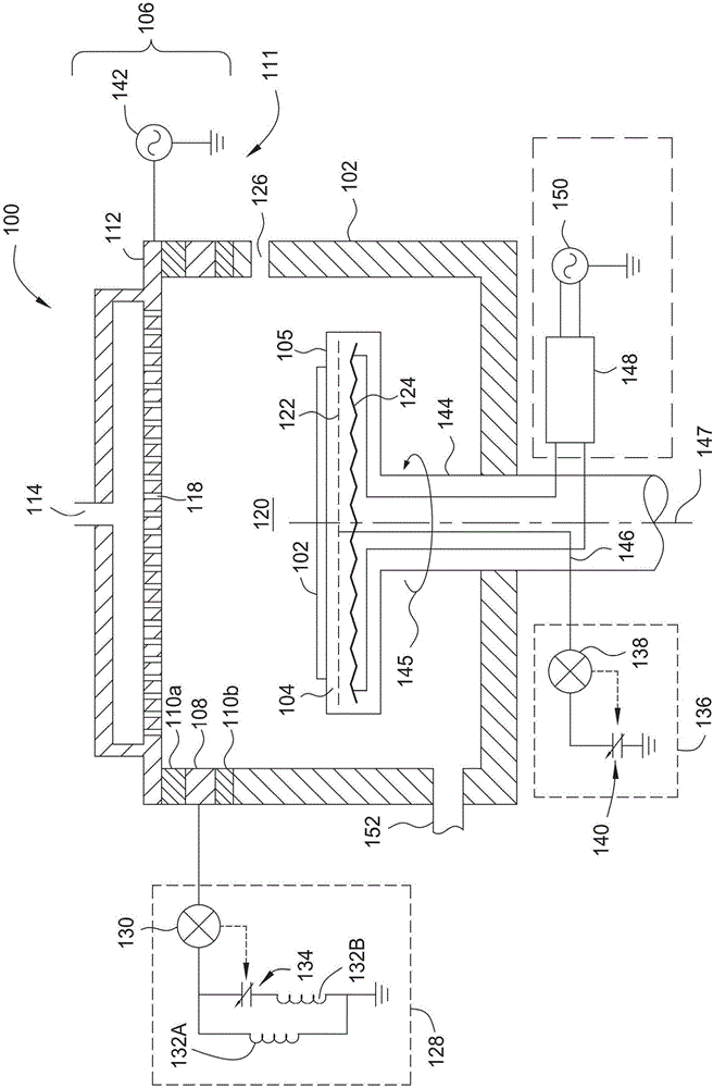
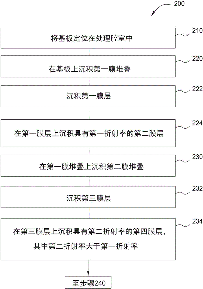
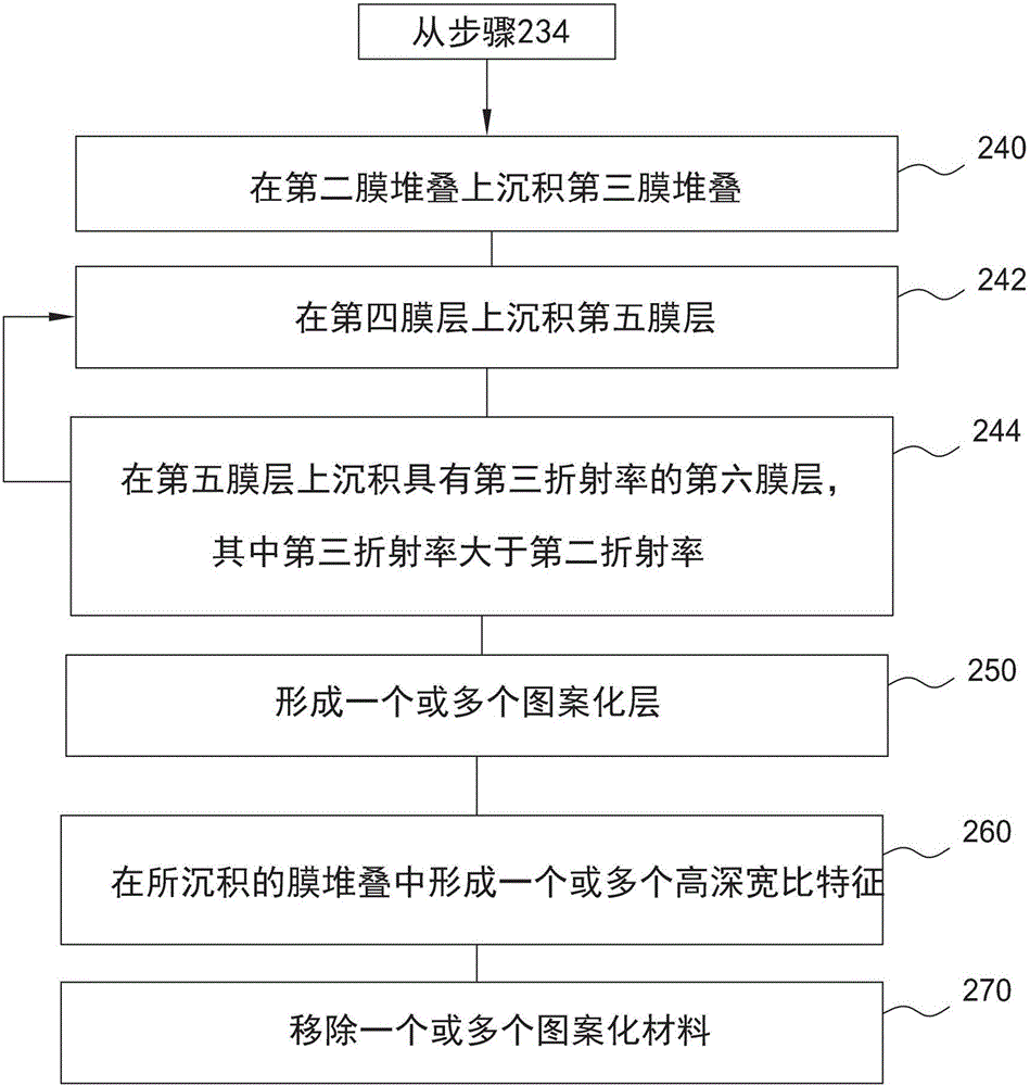
[0018] The following disclosure describes thin films having high aspect ratio features formed therein, processes for depositing the thin films and forming high aspect ratio features therein, and apparatus for accomplishing the above processes. in the description below and in the figure 1 Specific details are set forth through Figure 5 to provide a thorough understanding of various implementations of the present disclosure. Additional details describing well-known methods and systems commonly associated with the deposition of thin films are not set forth in the following disclosure in order to avoid unnecessarily obscuring the description of various implementations.

[0019] Many of the details, components, and other features described herein are merely illustrative of particular implementations. Accordingly, other implementations may have other details, components, and features without departing from the spirit or scope of the present disclosure. Additionally, additional im...


PUM

PropertyMeasurementUnit
thicknessaaaaaaaaaa
diameteraaaaaaaaaa
diameteraaaaaaaaaa

Abstract

Implementations of the present disclosure generally relate to thin films incorporating high aspect ratio feature definitions and methods for forming the same. As gate height increases, 3D NAND gate stacks are subject to higher aspect ratio etching. Due to the current limitations of etching techniques, the vertical etch profile typically tapers as the depth into the gate stack increases. The inventors have devised a unique deposition scheme that compensates for etch performance degradation in deep trenches by a novel plasma-enhanced chemical vapor deposition (PECVD) film deposition method. The inventors have found that by grading various properties (e.g., refractive index, stress of the film, dopant concentration in the film) of the as-deposited films (e.g., silicon nitride) a more uniform etch profile can be achieved by compensating for variations in both dry and wet etch rates.

Description

technical field [0001] Implementations of the present disclosure generally relate to thin films defined in conjunction with high aspect ratio features and methods of forming the same. Background technique [0002] As circuit density increases in next-generation devices, interconnects such as vias, trenches, contacts, gate structures, and other features, as well as the width of dielectric material between interconnects, will shrink in size down to 45nm and 32nm, while the thickness of the dielectric layer remains substantially constant, which results in an increased feature aspect ratio. To enable the fabrication of next-generation devices and structures, three-dimensional (3D) stacking of semiconductor chips is often utilized to improve transistor performance. By arranging transistors in three dimensions instead of the conventional two, multiple transistors can be arranged in close proximity to each other in an integrated circuit (IC). Three-dimensional (3D) stacking of se...

Claims


Application Information

Patent Timeline
Patent Type & Authority Applications(China)
IPC IPC(8): H01L21/02H01L21/311H01L21/28H01L21/8247H01L27/115H01L29/423
CPCH01L21/02164H01L21/0217H01L21/022H01L21/02274H01L21/31116H01L21/31144H01L29/42364H10B41/20H10B43/20C23C16/45523H01L21/02211H01L21/02216C23C16/401C23C16/345H10B41/27H10B43/27H01L21/0228H01L21/3065H01L21/32136
Inventor P·P·贾A·阔韩新海T·J·权金柏涵B·H·祁R·金S·H·金
Owner APPLIED MATERIALS INC
Why Eureka
Try Eureka