Wafer Level optoelectronic device packages and methods for making the same
A technology for optoelectronic devices and wafers, used in semiconductor/solid-state device manufacturing, electrical solid-state devices, electrical components, etc., can solve problems such as increased manufacturing cost, high yield, loss, etc., to achieve low cost, reduced bill of materials, and high yield. the effect of making
- Summary
- Abstract
- Description
- Claims
- Application Information
AI Technical Summary
Problems solved by technology
Method used
Image

Examples
Embodiment Construction
[0085] Exemplary embodiments of the present disclosure will be described in more detail below with reference to the accompanying drawings. Although exemplary embodiments of the present disclosure are shown in the drawings, it should be understood that the present disclosure may be embodied in various forms and should not be limited by the embodiments set forth herein. Rather, these embodiments are provided for more thorough understanding of the present disclosure and to fully convey the scope of the present disclosure to those skilled in the art.
[0086] Priority Application: This application claims priority over U.S. Patent Application No. 14 / 749,169, filed June 24, 2015, and U.S. Provisional Patent Application No. 62 / 148,575, filed April 16, 2015 right.
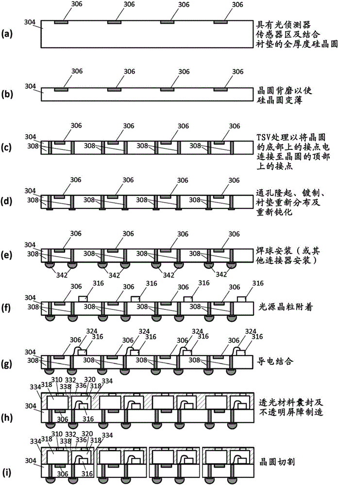
[0087] include section image 3 (a) to image 3 (i) image 3 It will now be used to illustrate the fabrication of optoelectronic devices (and, more particularly, a plurality of such devices) according to certain embodi...
PUM
 Abstract
Description
Claims
Application Information
 - R&D Engineer
- R&D Manager
- IP Professional
- Industry Leading Data Capabilities
- Powerful AI technology
- Patent DNA Extraction
Browse by: Latest US Patents, China's latest patents, Technical Efficacy Thesaurus, Application Domain, Technology Topic.
© 2024 PatSnap. All rights reserved.Legal|Privacy policy|Modern Slavery Act Transparency Statement|Sitemap