Circuit board compatible with crystal, and circuit thereof

A technology of circuit boards and crystals, which is applied to printed circuits, printed circuits, printed circuits connected with non-printed electrical components, etc., can solve the problems of space waste, reduce peripheral circuit devices, save space, reduce materials and cost effect

Active Publication Date: 2016-10-26
四川酷赛科技有限公司
View PDF5 Cites 4 Cited by
  • Summary
  • Abstract
  • Description
  • Claims
  • Application Information

AI Technical Summary

Problems solved by technology

[0006] In view of the shortcomings of the prior art above, the purpose of the present invention is to provide a crystal-compatible circuit board and its circuit to solve the problem of waste of space caused by the simultaneous arrangement of single crystal and double crystal on the existing circuit board

Method used


Image

  • Circuit board compatible with crystal, and circuit thereof
  • Circuit board compatible with crystal, and circuit thereof
  • Circuit board compatible with crystal, and circuit thereof

Examples


Embodiment Construction

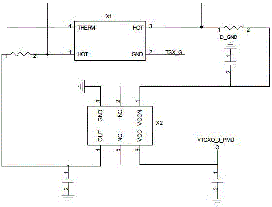
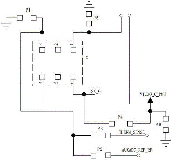
[0025] The invention provides a crystal-compatible circuit board and its circuit. Aiming at the limited space of the circuit board and the shortage of resources, circuits and circuits compatible with more crystal sizes are designed to maximize the utilization of cost and resources. In order to make the object, technical solution and advantages of the present invention more clear and definite, the present invention will be further described in detail below with reference to the accompanying drawings and examples. It should be understood that the specific embodiments described here are only used to explain the present invention, not to limit the present invention.

[0026] Please also see figure 2 with image 3 The crystal compatible circuit board provided by the present invention is provided with a crystal pad for welding single crystal or double crystal, and several device pads for welding peripheral circuit devices of single crystal and double crystal. The plurality of dev...


PUM


Abstract

The invention discloses a circuit board compatible with a crystal, and a circuit thereof. The circuit board comprises a CPU bonding pad and a CPU crystal oscillator bonding pad. The circuit board also comprises a crystal bonding pad for welding a single crystal or bicrystal, and a plurality of device bonding pads for welding single crystal and bicrystal peripheral circuits. The plurality of device bonding pads are connected with the crystal bonding pad through wires, and the crystal bonding pad is connected with the CPU bonding pad and the CPU crystal oscillator bonding pad. Because only one crystal bonding pad is set and the device bonding pads for the single crystal and bicrystal peripheral circuits are set at the same time, the single crystal or bicrystal for welding can be welded on the crystal bonding pad according to the actual needs. A corresponding device is selected for welding pasters on the device bonding pads or suspension, thereby forming a peripheral circuit corresponding to the crystal. One circuit board can be compatible with the single crystal and bicrystal and the peripheral circuits thereof. Compared with the prior art, the circuit board reduces one crystal and the corresponding peripheral circuit thereof, saves the space, and reduces the material and cost.

Description

technical field [0001] The invention relates to the technical field of X-ray machine movement, in particular to a crystal-compatible circuit board and its circuit. Background technique [0002] With the rapid development of GPS (Global Positioning System, Global Positioning System), WLAN (Wireless Local Area Network), LTE (Long Term Evolution, long-term evolution) and other technologies, high-performance crystals with excellent long-term and short-term frequency stability for radio frequency communication systems Demand for oscillators has also skyrocketed. Because the temperature compensated crystal oscillator (TCXO, referred to as crystal oscillator) is one of the key devices in the radio frequency circuit of portable communication terminals such as mobile phones, it includes a voltage-controlled temperature-compensated crystal oscillator (VCTCXO, referred to as temperature-compensated crystal with voltage-controlled frequency correction function) ) can cooperate with the...

Claims


Application Information

Patent Timeline
IPC IPC(8): H05K1/02H05K1/11H05K1/18
CPCH05K1/0296H05K1/116H05K1/18H05K2201/10098
Inventor 刘海山
Owner 四川酷赛科技有限公司
Why Eureka
Try Eureka