Binary channel RC-LIGBT device and manufacturing method therefor

A dual-channel, device technology, used in semiconductor/solid-state device manufacturing, semiconductor devices, electrical components, etc., can solve the problems affecting the stability and reliability of LIGBT devices, the PN junction cannot be normally turned on, and the PN junction conduction voltage drop increases. and other problems, to achieve the effect of improving stability and reliability, low conduction voltage drop, and strong freewheeling ability

Inactive Publication Date: 2016-11-02
UNIV OF ELECTRONICS SCI & TECH OF CHINA
View PDF4 Cites 18 Cited by
  • Summary
  • Abstract
  • Description
  • Claims
  • Application Information

AI Technical Summary

Problems solved by technology

Under low temperature conditions, the turn-on voltage drop of the PN junction formed by the P-type collector region 8 and the N-type electric field cut-off region 7 increases, and it needs to be turned on under a larger current condition, resulting in a more obvious negative resistance phenomenon. , and even cause the PN junction formed by the P-type collector region 8 and the N-type electric field stop region 7 in the device to fail to open normally, which seriously affects the stability and reliability of LIGBT devices

Method used


Image

  • Binary channel RC-LIGBT device and manufacturing method therefor
  • Binary channel RC-LIGBT device and manufacturing method therefor
  • Binary channel RC-LIGBT device and manufacturing method therefor

Examples


Embodiment 1

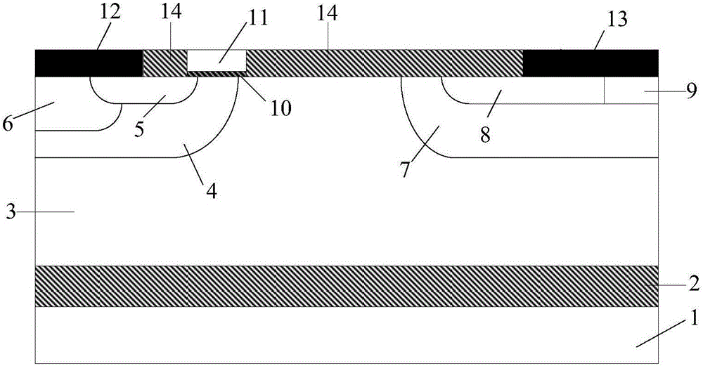
[0035] This embodiment provides a dual-channel RC-LIGBT device with a voltage level of 400V, and its cell structure is as follows figure 2 As shown, it includes a substrate 1, a silicon oxide dielectric layer 2 on the substrate 1, an N-type drift region 3 on the silicon oxide dielectric layer 2, an emitter structure on the N-type drift region 3, a gate structure, A collector structure and a dielectric layer 14; the emitter structure is composed of a P-type base region 4, an N+ source region 5, a P+ contact region 6 and a metal emitter 12, wherein the P-type base region 4 is arranged in the N-type drift region 3 and located on the left side of its top, the P+ contact region 6 and the N+ source region 5 are independently arranged in the P-type base region 4, and the front surfaces of the P+ contact region 6 and the N+ source region 5 are in contact with the metal emitter 12; The gate structure is located on the right side of the emitter structure and is composed of a gate diele...

Embodiment 2

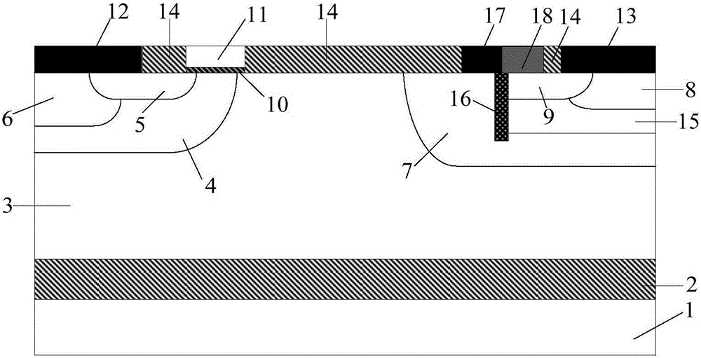
[0038] This embodiment provides a dual-channel RC-LIGBT device with a voltage level of 400V, and its cell structure is as follows image 3 As shown, it includes a substrate 1, a silicon oxide dielectric layer 2 on the substrate 1, an N-type drift region 3 on the silicon oxide dielectric layer 2, an emitter structure on the N-type drift region 3, a gate structure, A collector structure and a dielectric layer 14; the emitter structure is composed of a P-type base region 4, an N+ source region 5, a P+ contact region 6 and a metal emitter 12, wherein the P-type base region 4 is arranged in the N-type drift region 3 and located on the left side of its top, the P+ contact region 6 and the N+ source region 5 are independently arranged in the P-type base region 4, and the front surfaces of the P+ contact region 6 and the N+ source region 5 are in contact with the metal emitter 12; The gate structure is located on the right side of the emitter structure and is composed of a gate dielec...


PUM


Abstract

A binary channel RC-LIGBT device and a manufacturing method therefor are disclosed. The invention belongs to the field of power semiconductor integrated circuits and specifically relates to a reverse conducting-LIGBT / RC-LIGBT and a manufacturing method therefor that are used for suppressing snapback phenomena of a conventional RC-LIGBT device, improving characteristics of backward diodes and improving device stability and reliability. The RC-LIGBT device disclosed in the invention has a unilateral electric conduction path having binary channels, the unilateral electric conduction path is formed by introducing a composite structure at a collector electrode end of the device, impact exerted on conduction characteristics by an N type collecting zone can be completely shielded in a forward direction LIGBT work mode, the snapback phenomena can be completely eliminated, the RC-LIGBT device disclosed in the invention has the same low conduction voltage drop as the conventional LIGBT, device stability and reliability can be improved, two freewheel channels are provided at the collector electrode end in a backward diode freewheel work mode, freewheeling capacity of the RC-LIGBT device is optimized, and the RC-LIGBT device is enabled to have a small conduction voltage drop.

Description

technical field [0001] The invention belongs to the field of power semiconductor integrated circuits, and relates to a lateral insulated gate bipolar transistor (Lateral Insulated Gate Bipolar Transistor, LIGBT), in particular to a lateral reverse conduction type insulated gate bipolar transistor (Reverse Conducting-LIGBT, RC-LIGBT) and its preparation method. Background technique [0002] Lateral Insulated Gate Bipolar Transistor (LIGBT) is a new type of device in power integrated circuits. It not only has the advantages of LDMOSFET easy to drive, simple control, and easy integration, but also has the advantages of reduced conduction voltage of power transistors, large on-state current, and low loss. It has become one of the core devices of modern power semiconductor integrated circuits. Literature (Shigeki T., Akio N., Youichi A., Satoshi S. and Norihito T. Carrier-Storage Effect and Extraction-Enhanced Lateral I GBT (E 2 LIGBT): A Super-High Speed ​​and Low On-state Vol...

Claims


Application Information

Patent Timeline
Patent Type & Authority Applications(China)
IPC IPC(8): H01L29/739H01L21/331
CPCH01L29/66325H01L29/7393
Inventor 张金平黄孟意李丹底聪刘竞秀李泽宏任敏张波
Owner UNIV OF ELECTRONICS SCI & TECH OF CHINA
Why Eureka
Try Eureka