System-in-package chip and preparation method thereof and device having chip

A system-in-package and chip technology, applied in the field of microelectronics, can solve problems such as difficult to meet the needs of the Internet of Things

Inactive Publication Date: 2016-11-09
MIDEA SMART TECH CO LTD +1
View PDF7 Cites 3 Cited by
  • Summary
  • Abstract
  • Description
  • Claims
  • Application Information

AI Technical Summary

Problems solved by technology

[0005] However, with the continuous demand of the Internet of Things for chips in all aspects of their performance, figure 1 The SiP modules shown are increasingly difficult to meet the needs of the Internet of Things

Method used


Image

  • System-in-package chip and preparation method thereof and device having chip
  • System-in-package chip and preparation method thereof and device having chip
  • System-in-package chip and preparation method thereof and device having chip

Examples


Embodiment Construction

[0046] Specific embodiments of the present invention will be described in detail below in conjunction with the accompanying drawings. It should be understood that the specific embodiments described here are only used to illustrate and explain the present invention, and are not intended to limit the present invention.

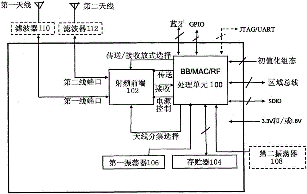
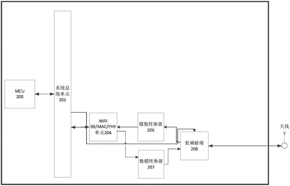
[0047] figure 2 A block diagram of a SiP module provided for an embodiment of the present invention. Such as figure 2 As shown, the SiP module provided by an embodiment of the present invention includes: a radio frequency front-end module 208; an analog-to-digital converter 206 and a digital-to-analog converter 207; a microcontroller processing unit 200; a system bus unit 201; and a wireless fidelity (WiFi) Base Band / Media Access Control / Radio Frequency (Base Band / Media Access Control / Radio Frequency; BB / MAC / PHY) unit 204, and the microcontroller processing unit (Mirco Controller Unit; MCU) 200 via the system bus unit 201 Connected, used to perform one or m...


PUM


Abstract

The invention relates to the field of microelectronics and discloses a system-in-package chip, a device having the system-in-package chip and a preparation method of the system-in-package chip. The system-in-package chip comprises a radio frequency front-end module, an analog-digital converter, a digital-analog converter, a microcontroller processing unit, a system bus unit and a Wifi BB / MAC / PHY unit, wherein the Wifi BB / MAC / PHY unit is connected with the microcontroller processing unit through the system bus unit and is used for carrying out one or more step of the following steps: after carrying out digital-to-analogue conversion on the signal from the microcontroller processing unit through the analog-digital converter, sending the signal out through the radio frequency front-end module; and receiving the signal obtained after carrying out digital-to-analogue conversion through the analog-digital converter on the signal received by the radio frequency front-end module, and sending the signal to the microcontroller processing unit. Through the technical scheme above, high-speed operation can be achieved, data throughput is high, and design of hardware is simplified.

Description

technical field [0001] The invention relates to the field of microelectronics, in particular to a system-in-package chip, a device containing the system-in-package chip, and a preparation method of the system-in-package chip. Background technique [0002] The Internet of Things (Internet of Things) is an important part of the new generation of information technology, and the Internet of Things is the Internet where things are connected. It uses communication technologies such as local networks or the Internet to connect sensors, controllers, machines, people and things together in a new way, forming a connection between people and things, things and things, and realizing informatization, remote management control and intelligence. network of. It is a ubiquitous network built on the Internet. The important foundation and core of the Internet of Things technology is still the Internet. Through the integration of various wired and wireless networks and the Internet, the infor...

Claims


Application Information

Patent Timeline
Patent Type & Authority Applications(China)
IPC IPC(8): H01L25/18H01L21/60H04B1/40H04W88/06
CPCH01L24/83H01L24/85H01L24/92H01L25/18H01L2224/83024H01L2224/8321H01L2224/83815H01L2224/85801H01L2224/92147H04B1/40H04W88/06
Inventor 梁海浪
Owner MIDEA SMART TECH CO LTD
Why Eureka
Try Eureka