Novel GaN-based HEMT device with gate structure

A gate structure and a new type of technology, applied in the field of GaN-based HEMT devices, can solve the problems of not increasing the on-resistance of the device, increasing the on-resistance, reducing the device performance, etc., to improve reliability and service life, improve breakdown voltage, The effect of suppressing the current collapse effect

Pending Publication Date: 2016-11-09
上海华时嘉库半导体有限公司
View PDF4 Cites 2 Cited by
  • Summary
  • Abstract
  • Description
  • Claims
  • Application Information

AI Technical Summary

Problems solved by technology

Due to the current collapse effect of GaN HEMT devices during application, this effect can easily lead to device performance degradation, such as gain, RF output power, efficiency, etc. Improving the device current collapse effect is a feasible way to improve device performance
The reliability and performance of GaN devices are a pair of contradictory systems. Improving the reliability of the device can be achieved by increasing the breakdown voltage of the device, and increasing the breakdown voltage of the device will generally lead to an increase in the on-resistance of the device, thereby reducing the device's performance, how to improve the breakdown voltage of the device without increasing the on-resistance of the device has become an urgent problem to be solved

Method used


Image

  • Novel GaN-based HEMT device with gate structure
  • Novel GaN-based HEMT device with gate structure

Examples


Embodiment Construction

[0012] The following will clearly and completely describe the technical solutions in the embodiments of the present invention with reference to the accompanying drawings in the embodiments of the present invention. Obviously, the described embodiments are only some, not all, embodiments of the present invention. Based on the embodiments of the present invention, all other embodiments obtained by persons of ordinary skill in the art without making creative efforts belong to the protection scope of the present invention.

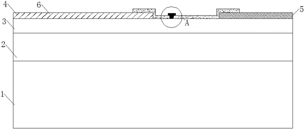
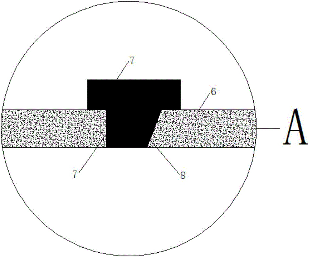
[0013] see Figure 1-2 , the present invention provides a technical solution: a GaN-based HEMT device with a novel gate structure, including a substrate 1, the substrate 1 is SiC, the upper end of the substrate 1 is provided with a channel layer 2, and the upper end of the channel layer 2 A barrier layer 3 is provided, the thickness of the channel layer 2 is 0.5-5um, the thickness of the barrier layer 3 is 5-500um, and the source electrode 4 and the drain elec...


PUM


Abstract

The invention discloses a novel GaN-based HEMT device with a gate structure. The upper end of an insulating layer is provided with a jack in the shape of an inverted right trapezoid between a source electrode and a drain electrode. A bottom layer gate electrode in the shape of a right trapezoid is inserted into the jack correspondingly. A top layer gate electrode is arranged on the upper end of the bottom layer gate electrode. The bottom layer gate electrode of the device is of a right trapezoid structure, so that the distance between the bottom layer gate electrode and a barrier layer is increased in a stepped manner rather than suddenly. The structure can increase the breakdown voltage of the device without increasing the distance between the gate electrode and the drain electrode. Meanwhile, as the right bottom angle near the drain electrode end of the bottom layer gate electrode does not form a right angle, the thermoelectronic effect of the device can be reduced, so that the reliability and service life of the device can be improved. Besides, the current collapse effect of the device can be better inhibited through reducing the distance between the top layer gate electrode and the barrier layer.

Description

technical field [0001] The invention relates to the technical field of GaN-based HEMT devices, in particular to a GaN-based HEMT device with a novel gate structure. Background technique [0002] As the third-generation semiconductor material representative of GaN-based HEMT (High Electron Mobility Transisors) devices, it has the advantages of high breakdown electric field, high mobility, large band gap, strong radiation resistance, and good thermal conductivity. These excellent properties of GaN These irreplaceable advantages make GaN a research hotspot, and have broad application prospects in microwave radio frequency and high power. With the advent of the 5G era, LDMOS (Lateral Double-Diffused Metal-Oxide Semiconductor) will not be able to meet the high-frequency, broadband, and high-efficiency requirements of base station power amplifier systems. It is urgent to develop a new generation of GaN HEMT devices to replace LDMOS devices in base stations. need. Due to the curr...

Claims


Application Information

Patent Timeline
Patent Type & Authority Applications(China)
IPC IPC(8): H01L29/778H01L29/423H01L29/06
CPCH01L29/06H01L29/0611H01L29/423H01L29/42316H01L29/778
Inventor 李宝国马京路韩威张书敬张达泉孙丞杨荣
Owner 上海华时嘉库半导体有限公司
Why Eureka
Try Eureka