Polycrystalline silicon semi-melting ingot casting method

A polysilicon ingot furnace and polysilicon technology, applied in the growth of polycrystalline materials, chemical instruments and methods, crystal growth, etc., can solve the problems of unguaranteed quality of ingot finished products, poor impurity removal effect, etc., and achieve preheating and melting process Easy to master, convenient to realize, and simple processing steps

Inactive Publication Date: 2016-11-16
XIAN HUAJING ELECTRONICS TECH
View PDF10 Cites 4 Cited by
  • Summary
  • Abstract
  • Description
  • Claims
  • Application Information

AI Technical Summary

Problems solved by technology

[0005] The technical problem to be solved by the present invention is to provide a polysilicon semi-melted ingot casting method for the above-mentioned deficiencies in the prior art. There are problems such as poor impurity removal effect and ingot quality cannot be guaranteed

Method used


Image

  • Polycrystalline silicon semi-melting ingot casting method
  • Polycrystalline silicon semi-melting ingot casting method
  • Polycrystalline silicon semi-melting ingot casting method

Examples


Embodiment 1

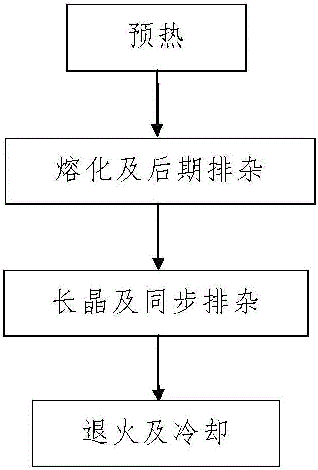
[0055] Such as figure 1 A kind of polysilicon semi-melting ingot casting method shown, comprises the following steps:

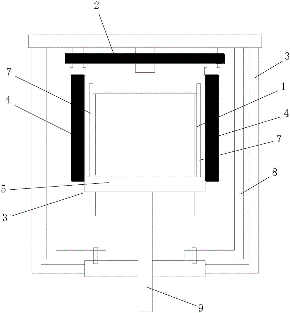
[0056] Step 1. Preheating: Turn on the top heater 2 located above the crucible 1 in the polysilicon ingot furnace 3 and the four side heaters 4 respectively arranged outside the four side walls of the crucible 1, and use polysilicon ingots Furnace 3 preheats the silicon material loaded in crucible 1, and gradually raises the heating temperature of polysilicon ingot casting furnace 3 to T1; the preheating time is 5 hours, where T1=1200°C;

[0057] In this step, the top-side ratio coefficient c=1 of the polysilicon ingot furnace 3;

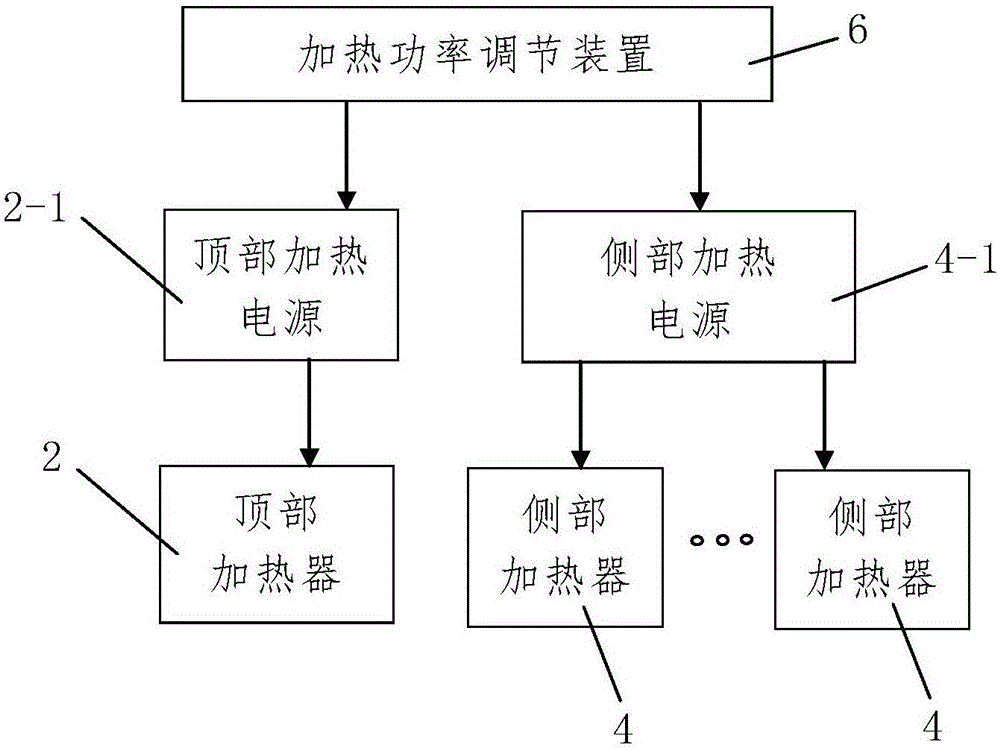
[0058] Among them, the top-side ratio coefficient c ding is the power ratio coefficient of top heater 2 and P d is the actual heating power of top heater 2, P d max is the maximum heating power of the top heater 2; P c is the actual heating power of the side heater 4, P c max is the maximum heating power of the side hea...

Embodiment 2

[0109] In this example, the difference from Example 1 is: T1=1125°C in step 1, the preheating time is 6h, and P d max 150kW, P c max =220kW; T2=1530 DEG C in the step 201, heat preservation 8h when carrying out the first time heat preservation in the step 2012, heat preservation 14h when carrying out the second heat preservation in the step 2013; Continue melting time in the step 202 is 40min, T3=1420 DEG C; step T4=1410°C in the third step, c in step 301 1 =0.9, c 0 =0.6, the crystal growth time in the early stage is 15h; in step 302, T5=1405°C, and the crystal growth time in the later stage is 35h; the crystal growth rate in step 3 is controlled at 10mm / h; the Q1 described in step 1, step 2 and step 3 = 550 mbar.

[0110] In this embodiment, the remaining method steps and process parameters are the same as those in Embodiment 1.

[0111] In this embodiment, the surface of the processed polysilicon ingot has no impurities, no sticky pot phenomenon, the oxygen content at t...

Embodiment 3

[0113] In this example, the difference from Example 1 is: in step 1, T1=1285°C, the preheating time is 4h, and the P d max 180kW, P c max =260kW; T2=1550 DEG C in the step 201, insulate 4h when carrying out the first time insulation in the step 2012, insulate 10h when carrying out the second insulation in the step 2013; Continue melting time in the step 202 is 15min, T3=1440 DEG C; step T4=1430°C in the third step, c in step 301 1 =0.8,c 0 =0.3, the crystal growth time in the early stage is 10h; in step 302, T5=1425°C, and the crystal growth time in the later stage is 28h; the crystal growth rate in step 3 is controlled at 13mm / h; the Q1 described in step 1, step 2 and step 3 = 650 mbar.

[0114] In this embodiment, the remaining method steps and process parameters are the same as those in Embodiment 1.

[0115] In this embodiment, the surface of the processed polysilicon ingot has no impurities, no sticky pot phenomenon, the oxygen content at the bottom of the ingot is re...


PUM


Abstract

The present invention discloses a polycrystalline silicon semi-melting ingot casting method, comprising the steps of first, preheating: using a polycrystalline silicon ingot furnace to preheat silicon material charged in a crucible, with a top-side ratio coefficient c of the polycrystalline silicon ingot furnace being 1; second, melting and discharging impurities later: 201, melting; 202, discharging impurities in later stage of melting; using the polycrystalline silicon ingot furnace to continuously melt the silicon material for 15-40 min; during melting, adjusting heating power of a top heater and/or four side heaters so as to obtain 0.8>/=c<1; third, growing crystal and discharging impurities at the same time; during crystal growth, adjusting the heating power of the top heater and/or four side heaters so as to obtain 0.3</=c<0.9; fourth, annealing and cooling. The method of the invention has simple steps and reasonable design, is convenient to implement and effective to use, and may provide a solution to the problems that existing polycrystalline silicon semi-melting ingot casting process has poor impurity-discharging effect and inability to ensure quality of finished ingots.

Description

technical field [0001] The invention belongs to the technical field of polycrystalline silicon ingot casting, and in particular relates to a method for semi-melting polycrystalline silicon ingot casting. Background technique [0002] Photovoltaic power generation is one of the most important clean energy sources with great development potential. The key factors restricting the development of photovoltaic industry are low photoelectric conversion efficiency on the one hand and high cost on the other hand. Photovoltaic silicon wafers are the basic material for the production of solar cells and components. The purity of polysilicon used to produce photovoltaic silicon wafers must be above 6N (that is, the total content of non-silicon impurities is below 1ppm), otherwise the performance of photovoltaic cells will be greatly negative influences. In recent years, the production technology of polycrystalline silicon wafers has made remarkable progress, and the polycrystalline ing...

Claims


Application Information

Patent Timeline
Patent Type & Authority Applications(China)
IPC IPC(8): C30B28/06C30B29/06
CPCC30B28/06C30B29/06
Inventor 李建军刘波波贺鹏蔺文虢虎平
Owner XIAN HUAJING ELECTRONICS TECH
Why Eureka
Try Eureka