

Method for forming 3D NAND flash memory
A flash memory and graphics technology, applied in the manufacturing of electrical components, electro-solid devices, semiconductor/solid-state devices, etc., can solve the problems of increased process difficulty, no advantages of 1YNAND products, and increased product reliability requirements, and can reduce the size, Increase process difficulty and improve the effect of equivalent storage area
- Summary
- Abstract
- Description
- Claims
- Application Information
AI Technical Summary
Problems solved by technology
Method used
Image

Examples
Embodiment Construction
[0028] The present invention will be further described below in conjunction with the accompanying drawings and specific embodiments, but not as a limitation of the present invention.
[0029] Such as figure 1 As shown, the present embodiment relates to a method for forming a 3D NAND flash memory, and the method specifically includes the following steps:
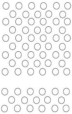
[0030] In step S1, a photomask is provided, and in the photomask, a predetermined number of rows of vertical hole patterns are formed in a row of gate lines; preferably, the predetermined number of rows is 9 rows, that is, in the photomask, In a row of gate lines, 9 rows of vertical hole patterns are formed, such as image 3 structure shown.
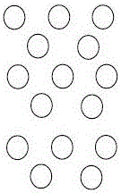
[0031] figure 2 It is a schematic structural diagram of an existing photomask forming vertical holes. It is obvious that the arrangement of vertical holes formed by the photomask in this embodiment is more optimized, which can save area and increase storage density.
[0032] In ste...
PUM
 Abstract
Description
Claims
Application Information