Eureka AIR delivers breakthrough ideas for toughest innovation challenges, trusted by R&D personnel around the world.

Bidirectional integrated embedded-type POP packaging structure and manufacturing method thereof

A packaging structure and manufacturing method technology, which is applied in semiconductor/solid-state device manufacturing, electrical components, electrical solid-state devices, etc., can solve problems such as poor electrical properties, easily deformed substrate thickness, unfavorable packaging integration, etc., and achieve high support strength , better electrical and heat dissipation performance, and better product performance

Inactive Publication Date: 2016-11-16
江阴芯智联电子科技有限公司
View PDF5 Cites 0 Cited by
  • Summary
  • Abstract
  • Description
  • Claims
  • Application Information

AI Technical Summary

Problems solved by technology

The current traditional three-dimensional packaging structure such as figure 1 As shown, the production method is to embed passive and active components on one side of the substrate, press or coat insulating materials, and use laser drilling and electroplating blind hole technology to lead the underlying functions to the second connection layer and then make the circuit layer. It still has the following disadvantages: the conventional substrate is easily deformed and thick, which is not conducive to improving the packaging integration; the laser drilling and electroplating blind hole process has low precision and poor heat dissipation and electrical properties, especially for high-frequency and high-power products.

Method used


Image

  • Bidirectional integrated embedded-type POP packaging structure and manufacturing method thereof
  • Bidirectional integrated embedded-type POP packaging structure and manufacturing method thereof
  • Bidirectional integrated embedded-type POP packaging structure and manufacturing method thereof

Examples


Embodiment Construction

[0046] The present invention will be further described in detail below in conjunction with the accompanying drawings and embodiments.

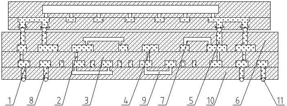
[0047] Such as figure 2 As shown, a bidirectional integrated embedded POP package structure in this embodiment includes a first package body and a second package body, the first package body includes a first circuit layer 1, and the first circuit layer 1. A first connection copper post 2 is provided on the front side. The first circuit layer 1 and the first connection copper post 2 are surrounded by a first insulating material 3. The front side of the first insulating material 3 is provided with a second circuit layer 4. , the front of the second circuit layer 4 is provided with a second connection copper column 5 and a first component 7, and the second circuit layer 4, the second connection copper column 5 and the first component 7 are surrounded by a second Insulating material 6, the back of the first insulating material 3 is provided with...


PUM


Abstract

The invention relates to a bidirectional integrated embedded-type POP packaging structure and a manufacturing method thereof. The structure comprises a first packaging body and a second packaging body, wherein the first packaging body comprises a first circuit layer (1); the front surface of the first circuit layer (1) is provided with a first connection copper column (2); a first insulated material (3) packages the first circuit layer (1); the front surface of the first insulated material (3) is provided with a second circuit layer (4); the front surface of the second circuit layer (4) is provided with a second connection copper column (5) and a first element (7); a second insulated material (6) packages the second circuit layer (4); the back surface of the first insulated material (3) is provided with a third connection copper column (8) and a second element (9); and a third insulated material (10) packages the third connection copper column (8). Multi-layer bidirectional embedding can be realized, the surface mount number of passive devices is more, the substrate space can be effectively saved, and the packaging process integration is improved.

Description

technical field [0001] The invention relates to a two-way integrated embedded POP packaging structure and a manufacturing method thereof, belonging to the technical field of semiconductor packaging. Background technique [0002] With the development of electronic devices towards high functionality and miniaturization, the proportion of passive devices in electronic systems is also increasing. At present, passive devices are mainly surface-mounted, which not only occupies a large amount of space on the surface of the substrate, but also has a large number of solder joints on the surface and a long interconnection length, which greatly reduces the electrical performance and reliability of the system. In order to save the surface space of the circuit board / substrate and provide thinner, better performance, and more reliable electronic systems, surface mount passive devices are transformed into embeddable passive devices, and all active components are buried The ultimate three-...

Claims


Application Information

Patent Timeline
Patent Type & Authority Applications(China)
IPC IPC(8): H01L23/14H01L23/498H01L21/48H01L21/60
CPCH01L2224/16225H01L2924/15311H01L2924/19105H01L23/142H01L21/4853H01L23/49811H01L23/49838H01L24/81H01L2224/81365
Inventor 王新潮陈灵芝张凯郁科锋
Owner 江阴芯智联电子科技有限公司
Why Eureka
Eureka Blog
Learn More