A Method of Optimizing Wafer Edge Defects for CMOS Image Sensors

An image sensor and edge defect technology, used in semiconductor devices, electrical solid state devices, radiation control devices, etc., can solve the problems of bombarding silicon oxide, affecting yield, and online defects.

Active Publication Date: 2019-03-26
SHANGHAI HUALI MICROELECTRONICS CORP
View PDF3 Cites 0 Cited by
  • Summary
  • Abstract
  • Description
  • Claims
  • Application Information

AI Technical Summary

Problems solved by technology

However, due to the inherent characteristics of furnace tube growth, three 20*20mm standoffs 1 are required to support the wafer. The positions of the three support points 1 are in close contact with the back of the wafer, and silicon nitride cannot be grown, such as figure 1 As shown, the low-temperature silicon dioxide at the positions of the three standoffs 1 on the back of the wafer in the subsequent etching is exposed to the etching plasma
[0006] The low-temperature silicon dioxide material on the back is loose, and it is easy to be bombarded by plasma to produce silicon oxide. Under the flow of cooling helium gas on the back of the wafer, it will be driven and dropped on the surface of the wafer, causing online defects and affecting the yield.

Method used


Image

  • A Method of Optimizing Wafer Edge Defects for CMOS Image Sensors
  • A Method of Optimizing Wafer Edge Defects for CMOS Image Sensors
  • A Method of Optimizing Wafer Edge Defects for CMOS Image Sensors

Examples


Embodiment Construction

[0028] In order to make the content of the present invention clearer and easier to understand, the content of the present invention will be described in detail below in conjunction with specific embodiments and accompanying drawings.

[0029] The present invention adjusts the different angles of different wafers located in the etching chamber in multiple steps, and gradually removes the low-temperature silicon dioxide (LTO) material dropped during the etching process on the back of the CIS wafer, so that the etching chamber is independently generated from the defect source To the function of self-clearing, thereby greatly reducing online defects and improving product yield.

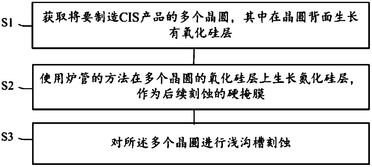
[0030] figure 2 A flow chart of a method for optimizing edge defects of a CMOS image sensor wafer according to a preferred embodiment of the present invention is schematically shown.

[0031] Such as figure 2 As shown, the method for optimizing CMOS image sensor wafer edge defects according to a prefe...


PUM


Abstract

The invention provides a method for optimizing wafer edge defects of a CMOS image sensor. The method comprises the following steps of: obtaining a plurality of wafers of a CIS product to be manufactured, wherein silicon oxide layers grows on the backs of the wafers; for the plurality of wafers of the CIS product to be manufactured, growing silicon nitride layers on the silicon oxide layers of the plurality of wafers with a furnace tube method as hard masks for subsequent etching; and carrying out shallow trench etching on the plurality of wafers.

Description

technical field [0001] The invention relates to the field of semiconductor manufacturing, and more specifically, the invention relates to a method for optimizing the edge defects of a CMOS image sensor wafer. Background technique [0002] CIS (CMOS Image Sensor, CMOS image sensor device) is a photoelectric conversion device that uses a row of built-in LED light-emitting diodes for illumination. Because of its small size and light weight, it is widely used in mobile devices such as smartphones with camera functions middle. [0003] The camera function of the contact sensor is particularly sensitive to the increase of electric leakage and white spots caused by metal pollution, especially the pollution of the working area, which leads to low yield and even scrapping of a large number of wafers. [0004] In order to prevent metal ion contamination on the back of the wafer during the process, a layer of silicon oxide is usually grown on the back of the CIS wafer. At present, loo...

Claims


Application Information

Patent Timeline
Patent Type & Authority Patents(China)
IPC IPC(8): H01L27/146
CPCH01L27/14683H01L27/14687
Inventor 许进唐在峰任昱吕煜坤
Owner SHANGHAI HUALI MICROELECTRONICS CORP
Why Eureka
Try Eureka