oled display device
A display device and light-emitting layer technology, which is applied in the field of OLED display devices, can solve the problems of brightness, contrast, inferior color, loss of light source efficiency, energy saving and three-primary-color independent pixel light-emitting technology, etc., to achieve cost saving, stability and life improvement Effect
- Summary
- Abstract
- Description
- Claims
- Application Information
AI Technical Summary
Problems solved by technology
Method used
Image
Examples
Embodiment 1
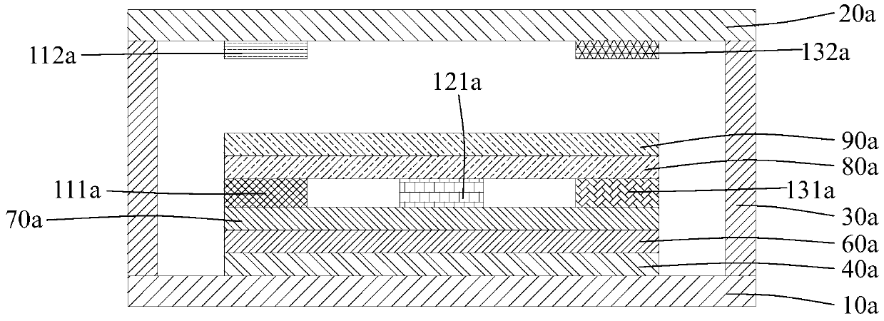
[0025] see figure 1 , figure 1 It is a schematic diagram of the first embodiment of the OLED display device of the present invention. Cooperate with reference figure 1 As shown, in the first embodiment, the OLED display device of the present invention includes: a substrate 10a and a cover plate 20a connected to each other by a sealant 30a, a sealed space 1a is formed between the substrate 10a and the cover plate 20a, and the sealed space 1a An anode layer 40a, a hole injection layer 60a, a hole transport layer 70a, an electron transport layer 80a, and a cathode layer 90a disposed on the substrate 10a, and a red particle disposed between the hole transport layer 70a and the electron transport layer 80a pixel, green subpixel, and blue subpixel. The sealant 30a can be sealed to protect the internal electronic devices. Preferably, the substrate 10a and the cover 20a are made of glass or flexible material, and at least one of the substrate 10a and the cover 20a is light-transmi...
Embodiment 2
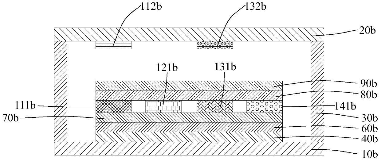
[0029] see figure 2 , figure 2 It is a schematic diagram of the second embodiment of the OLED display device of the present invention. Cooperate with reference figure 2 As shown, in the second embodiment, the OLED display device of the present invention includes: a substrate 10b and a cover plate 20b interconnected by a sealant 30b, a sealed space 1b is formed between the substrate 10b and the cover plate 20b, and the sealed space 1b The anode layer 40b, the hole injection layer 60b, the hole transport layer 70b, the electron transport layer 80b and the cathode layer 90b disposed on the substrate 10b, as well as the red sublayer disposed between the hole transport layer 70b and the electron transport layer 80b pixel, green subpixel, blue subpixel, and white subpixel. The sealant 30b can be sealed to protect the internal electronic devices. Preferably, the substrate 10b and the cover 20b are made of glass or a flexible material, and at least one of the substrate 10b and ...
PUM
 Abstract
Description
Claims
Application Information

