Semiconductor device and manufacturing method therefor

A manufacturing method and semiconductor technology, applied in the fields of semiconductor/solid-state device manufacturing, semiconductor devices, semiconductor/solid-state device components, etc., can solve the problems of technical difficulty, shallow depth, narrow width, etc., and achieve the effect of increasing the installation strength

Inactive Publication Date: 2016-11-30
TOWA
View PDF7 Cites 15 Cited by
  • Summary
  • Abstract
  • Description
  • Claims
  • Application Information

AI Technical Summary

Problems solved by technology

However, the concave portion 130 formed in the lead frame 112 has a narrow width and a shallow depth, so it is technical

Method used


Image

  • Semiconductor device and manufacturing method therefor
  • Semiconductor device and manufacturing method therefor
  • Semiconductor device and manufacturing method therefor

Examples


Embodiment 1

[0037] refer to Figure 1A ~ Figure 5B Embodiment 1 of the semiconductor device according to the present invention will be described. For ease of understanding, each drawing in this application is appropriately omitted or exaggerated and schematically drawn. Mark the same mark on the same structural element, and omit the description appropriately.

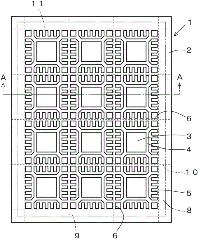
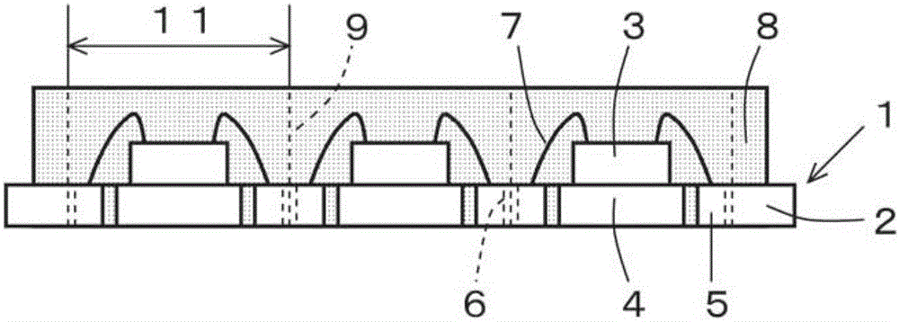
[0038] Such as Figure 1A As shown, the QFN substrate 1 is a to-be-cut object to be finally cut and separated into pieces. The QFN substrate 1 has a lead frame 2 . In the lead frame 2 , semiconductor chip mounting portions (die pads) 4 on which semiconductor chips (functional elements) 3 are respectively mounted are arranged in a matrix. The lead frame 2 contains metal such as copper (Cu) and 42 alloy (Fe—Ni). Lead-free metal plating or lead-free solder plating (not shown) is often formed in advance on the surface of the lead frame 2 . A large number of leads 5 serving as connection terminals for connection to the outside are...

Embodiment 2

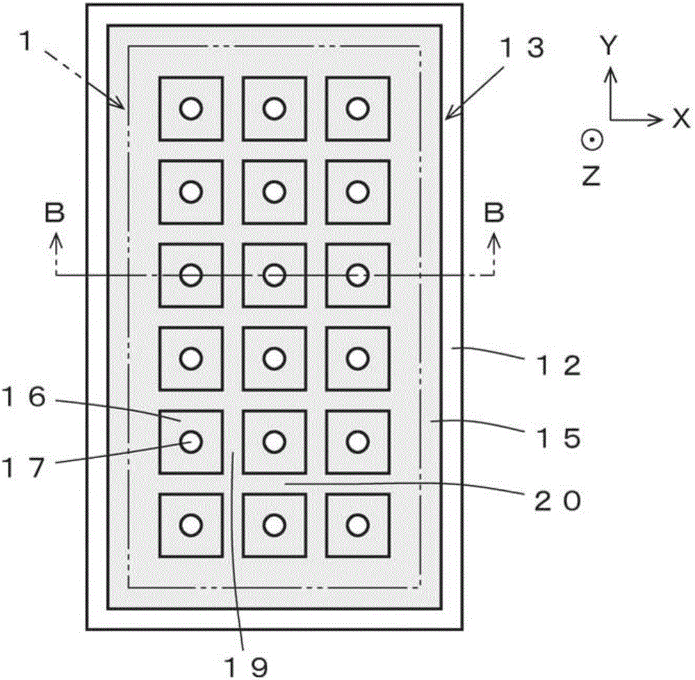
[0069] refer to Figure 6A , Figure 6B , Figure 7A , Figure 7B The method of performing the electroplating treatment on the QFN substrate 1 according to the present invention will be described respectively. Figure 6A , Figure 6B The illustrated QFN substrate 1 is a QFN substrate in which nine die pads 4 are arranged along the long-side direction and three die pads 4 are arranged along the short-side direction. Figure 6A , Figure 6B , Figure 7A , Figure 7B The illustrations of the lead wires are omitted.

[0070] about Figure 6AFor example, the cutting groove 22 (the portion indicated by the solid line in the figure) is formed in a portion where the sealing resin 8 is formed in a plan view (area surrounded by a dotted line in the figure). Therefore, the cutting grooves 22 are not formed in the offcut portions 32a, 32b, 32c, and 32d (portions indicated by hatching in the figure) included in the lead frame 2 . In this case, at one end of each dicing line (part...

Embodiment 3

[0078] refer to Figure 8 A dicing device used when manufacturing the semiconductor device according to the present invention will be described. Such as Figure 8 As shown, the dicing device 34A is, for example, a device for singulating the QFN substrate 1 to be cut into a plurality of QFN products 26 . The cutting device 34A includes a receiving unit A, a cutting unit B, and a delivery unit C as constituent elements, respectively. Each component (accepting unit A, cutting unit B, delivery unit C) is replaceable and can be attached and detached from other components.

[0079] The receiving unit A is provided with a preparation stand 35 . The QFN substrate 1 is received from the resin sealing device which is the device of the previous step. The QFN substrate 1 is arranged on the preparation table 35 with the sealing resin 8 side facing downward. The receiving unit A is provided with a control unit CTL that sets and controls the operation, cutting conditions, and the like of ...


PUM


Abstract

A semiconductor device and a manufacturing method therefor are provided. A cutting groove (22) is formed by cutting a predetermined thickness portion of a total thickness at a connecting strip of a lead wire frame (2) provided on a QFN substrate (1) with a rotary blade (21) thicker than a conventional rotary blade (24) ). Next, a plating layer (23) is formed on the bottom surface of the lead wire frame (2) and a surface of the cutting groove (22) via plating treatment. Next, the remaining thickness portion of the lead wire frame (2) at the cutting groove (22) and the total thickness portion of a sealing resin (8) are uniformly cut using the rotary blade (24) having a conventional thickness. The QFN substrate (1) is cut in two stages to completely remove the connecting bars, thereby manufacturing the QFN product (26). In the QFN product (26), the plating layer (23) can be stably formed on the bottom surface of a lead wire (5) and the surface of a concave portion (27) formed on a side surface of the lead wire (5).

Description

technical field [0001] The present invention relates to a semiconductor device called QFN (Quad Flat Non-leaded Package: Quad Flat Non-leaded Package) manufactured by singulating a diced object, and a method for manufacturing the same. Background technique [0002] Substrates including printed circuit boards and lead frames are virtually divided into multiple grid-like areas, chip-like components (such as semiconductor chips) are mounted in each area, and then the entire substrate is resin-sealed. The resulting substrate is called for sealed substrates. The sealed substrate is diced by a dicing mechanism such as a rotary knife, and is separated into individual pieces in units of regions, and the resulting products become products. [0003] Conventionally, a predetermined region of a sealed substrate has been cut by a cutting mechanism such as a rotary knife using a cutting device. First, a sealed substrate is placed on a dicing jig attached to a dicing table. Next, the se...

Claims


Application Information

Patent Timeline
IPC IPC(8): H01L21/78
CPCH01L21/78H01L2224/48091H01L2224/48247H01L2224/97H01L2924/181H01L2924/00014H01L2924/00012H01L21/288H01L21/76873H01L21/76874H01L23/3107H01L23/49551H01L23/49555H01L23/49582
Inventor 傳藤胜则片冈昌一石桥幹司
Owner TOWA
Why Eureka
Try Eureka