Flexible array substrate and its preparation method, flexible display device

A flexible array and flexible substrate technology, applied in the field of flexible display devices, can solve problems such as cracking, poor connection performance, and falling off, and achieve the effects of improving falling off or cracking, enhancing connection performance, and improving flexibility

Active Publication Date: 2019-04-05
WUHAN CHINA STAR OPTOELECTRONICS TECH CO LTD
View PDF3 Cites 0 Cited by
  • Summary
  • Abstract
  • Description
  • Claims
  • Application Information

AI Technical Summary

Problems solved by technology

The bending of the flexible array substrate has less damage to the organic and metal materials, but the damage to the less flexible inorganic oxide is relatively serious, especially when it is bent to a small radius of curvature, it is easy to cause the above-mentioned Failures such as cracking and delamination of flexible array substrates of inorganic oxides
For the gate insulating layer 8, the gate insulating layer 8 can be patterned to reduce its coverage area to reduce stress, reduce cracking and peeling dislocation problems, but the mutual bonding between the interlayer dielectric layer 9 and the buffer layer 2 The area is large, and the connection performance between the two is poor. When the flexible array substrate is bent, the interlayer dielectric layer 9 is easy to fall off or break from the buffer layer 2, which affects the quality of the flexible array substrate.

Method used


Image

  • Flexible array substrate and its preparation method, flexible display device
  • Flexible array substrate and its preparation method, flexible display device
  • Flexible array substrate and its preparation method, flexible display device

Examples


Embodiment Construction

[0031] In order to make the object, technical solution and advantages of the present invention clearer, the specific implementation manners of the present invention will be described in detail below in conjunction with the accompanying drawings. Examples of these preferred embodiments are illustrated in the accompanying drawings. The embodiments of the invention shown in and described with reference to the drawings are merely exemplary, and the invention is not limited to these embodiments.

[0032] Here, it should also be noted that, in order to avoid obscuring the present invention due to unnecessary details, only the structures and / or processing steps closely related to the solution according to the present invention are shown in the drawings, and the related Other details are not relevant to the invention.

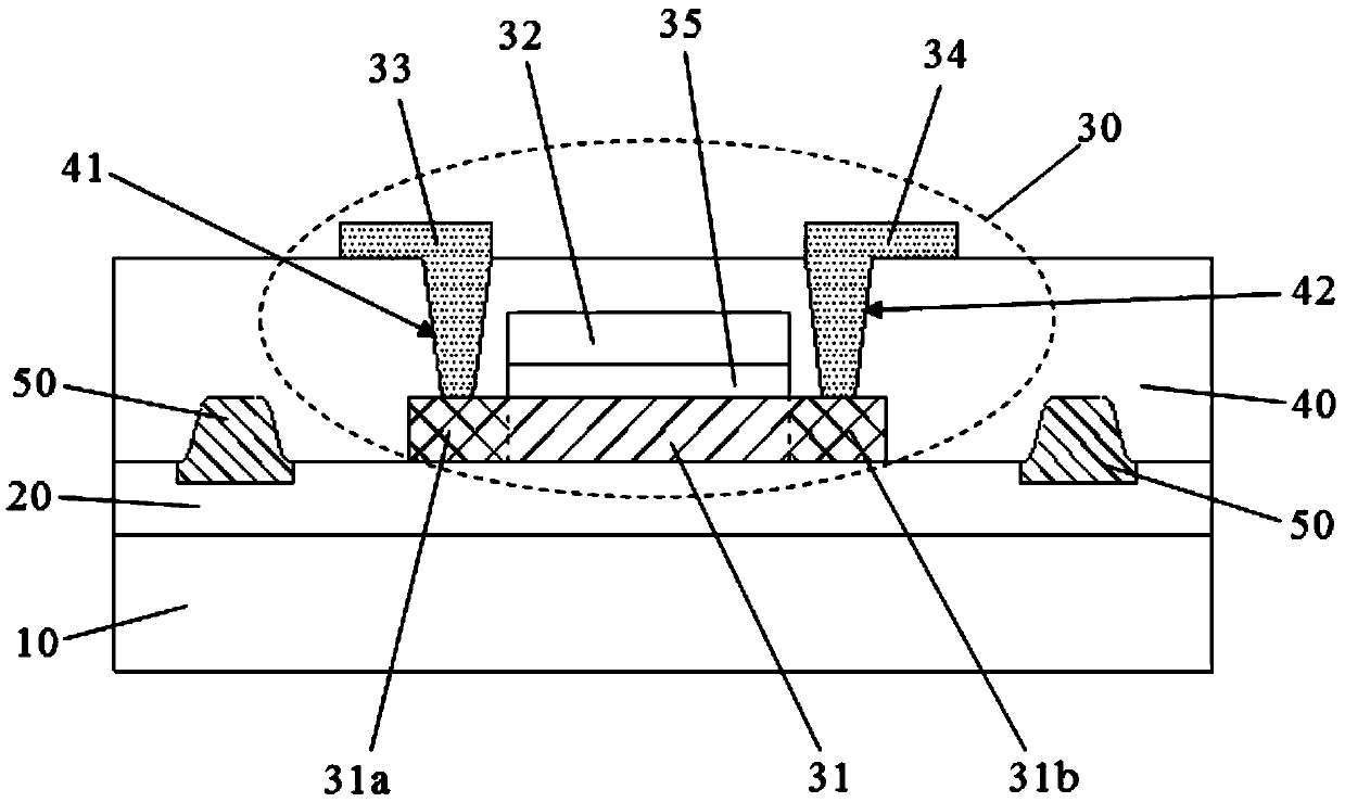
[0033] This embodiment first provides a flexible array substrate, such as figure 2 As shown, the flexible array substrate includes a flexible substrate 10 and a buf...


PUM


Abstract

The invention discloses a flexible array substrate, comprising a flexible substrate and a buffer layer on the flexible substrate, a plurality of thin film transistors are arranged in an array on the buffer layer, an interlayer dielectric layer is arranged on the thin film transistors, and the interlayer A dielectric layer covers the buffer layer; wherein, an interconnection structure is provided between the interlayer dielectric layer and the buffer layer, and at least one interconnection structure is respectively provided on both sides of each column of the thin film transistors, so The interconnecting structure member extends in a direction parallel to the bending axis of the flexible array substrate. The present invention also discloses the above-mentioned preparation method of the flexible array substrate and a flexible display device including the flexible array substrate. The invention enhances the connection performance of the interconnection structure layer in the flexible array substrate by arranging the interconnection structure member, improves the problem of peeling or cracking of the interconnection structure layer, and improves the quality of the flexible array substrate.

Description

technical field [0001] The present invention relates to the technical field of displays, in particular to a flexible array substrate and a preparation method thereof, and also to a flexible display device comprising the above flexible array substrate. Background technique [0002] Flat panel display technology has developed rapidly in the past ten years, and both the size of the screen and the quality of the display have made great progress. Flexible display devices can be used in many fields that require curved surface display due to their ability to bend, such as smart cards, electronic paper, smart labels, and various fields that traditional flat-panel display devices can apply to. Flexible display devices will definitely play an important role in the future display product market. With its fantastic and beautiful appearance, it occupies a huge market share. Generally, a flexible display device includes a stacked flexible array substrate and an electroluminescent device,...

Claims


Application Information

Patent Timeline
Patent Type & Authority Patents(China)
IPC IPC(8): H01L27/12H01L21/77H01L27/32
CPCH01L27/1218H01L27/1259H10K59/12Y02E10/549H01L29/78603H01L27/1244Y02P70/50H10K59/124H10K59/131H10K77/111H10K2102/311H10K10/468H10K50/15H10K50/16H10K50/81H10K50/82H10K71/00
Inventor 秦芳
Owner WUHAN CHINA STAR OPTOELECTRONICS TECH CO LTD
Why Eureka
Try Eureka