Touch substrate, manufacturing method of touch substrate and touch screen

A manufacturing method and substrate technology, applied in printed circuit, instrument, electrical digital data processing, etc., can solve the problems of black matrix pattern resistivity reduction, insulation performance degradation, permanent failure, etc., to improve ESD resistance and improve production Yield, the effect of reducing the risk of breakdown

Active Publication Date: 2016-12-07
BOE TECH GRP CO LTD +1
View PDF6 Cites 2 Cited by
  • Summary
  • Abstract
  • Description
  • Claims
  • Application Information

AI Technical Summary

Problems solved by technology

Electrostatic discharge may cause the performance of the internal components of the touch screen to deteriorate or break down to cause permanent failure, such as an open circuit or short circuit inside the touch screen
[0004] The existing touch substrate includes a touch area for touch detection and a black matrix pattern surrounding the touch area. The black matrix pattern is generally made of carbon balls. Usually the black matrix pattern has good insulation performance, but after multiple high-temperature After the process, the resistivity of the black matrix pattern decreases, and the insulation performance decreases, so that when the electrostatic charge of the device or the human body touches the touch electrodes that overlap the black matrix pattern, a huge discharge is instantaneously formed between different touch electrodes current, leading to the breakdown of the black matrix pattern, resulting in an open circuit or short circuit between the touch electrodes, resulting in poor touch performance or permanent failure of the corresponding area

Method used


Image

  • Touch substrate, manufacturing method of touch substrate and touch screen
  • Touch substrate, manufacturing method of touch substrate and touch screen
  • Touch substrate, manufacturing method of touch substrate and touch screen

Examples


Embodiment 1

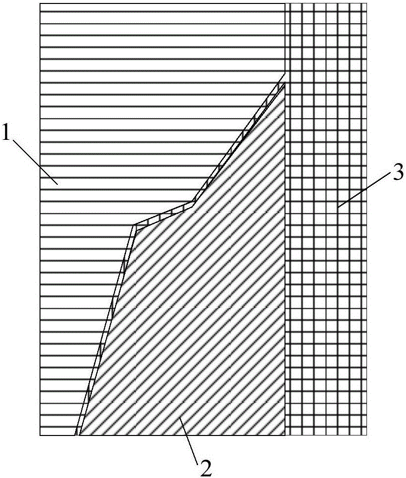
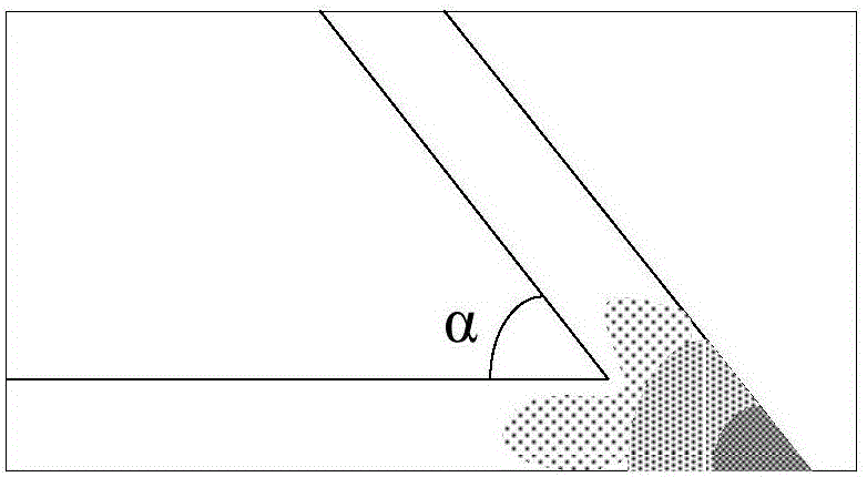
[0038] This embodiment provides a touch control substrate, including a touch control area and a black matrix pattern surrounding the touch area, the touch control substrate is provided with a plurality of touch electrode patterns, and the touch electrode patterns include overlapping In the first part on the black matrix pattern, the angle between any two adjacent sides of the first part is greater than a preset threshold.

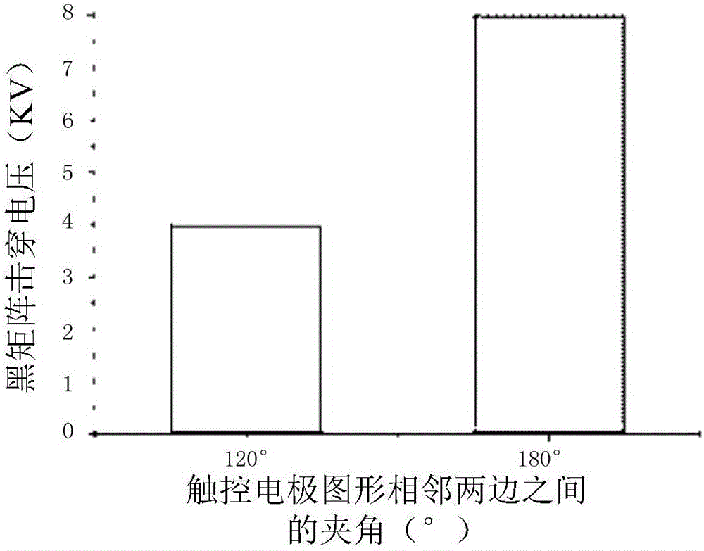
[0039] When the included angle between adjacent two sides of the touch electrode pattern overlapped on the black matrix pattern is small, the charge surface density at the tip of the touch electrode pattern is relatively large, and the electric field intensity is relatively high, so that the adjacent touch electrode patterns are easily separated. Electrostatic discharge occurs, causing the surrounding black matrix patterns to be broken down. After a lot of experimental verification, it is found that as the angle between the two adjacent sides of the touch e...

Embodiment 2

[0053] This embodiment also provides a touch screen, including the above-mentioned touch substrate, and the touch screen can be applied in a human-computer interaction device.

Embodiment 3

[0055] This embodiment provides a method for manufacturing a touch substrate, the touch substrate includes a touch area and a black matrix pattern surrounding the touch area, and the method includes:

[0056] A plurality of touch electrode patterns are formed, the touch electrode patterns include a first part overlapping the black matrix pattern, and the angle between any two adjacent sides of the first part is larger than a preset threshold.

[0057] When the included angle between adjacent two sides of the touch electrode pattern overlapped on the black matrix pattern is small, the charge surface density at the tip of the touch electrode pattern is relatively large, and the electric field intensity is relatively high, so that the adjacent touch electrode patterns are easily separated. Electrostatic discharge occurs, causing the surrounding black matrix patterns to be broken down. After a lot of experimental verification, it is found that as the angle between the two adjacent...


PUM


Abstract

The invention provides a touch substrate, a manufacturing method of the touch substrate and a touch screen, and belongs to the technical field of touch. The touch substrate comprises a touch area and a black matrix graphic which encircles the touch area; a plurality of touch electrode graphics are arranged on the touch substrate; each touch electrode graphic comprises a first part which is overlapped on the black matrix graphic; and the included angle between any two adjacent edges of each first part is greater than a preset threshold value. According to the technical scheme of the invention, the anti-ESD ability of the touch screen can be improved.

Description

technical field [0001] The invention relates to the field of touch technology, in particular to a touch substrate, a manufacturing method thereof, and a touch screen. Background technique [0002] In recent years, with the improvement of the controllability of mobile electronic devices and the development of electronic technology, touch screen technology has been widely used in electronic devices such as mobile phones, tablets, and notebook computers. In the development of touch technology, different technical directions such as resistance, capacitance, and electromagnetic have emerged. Capacitive touch screens have become mainstream products due to their low cost and excellent user experience. [0003] With the rapid growth of capacitive touch screens, people have higher and higher requirements for ESD (Electro-Static Discharge, electrostatic discharge) performance of touch products. Electrostatic discharge may cause the performance of the internal components of the touch ...

Claims


Application Information

Patent Timeline
Patent Type & Authority Applications(China)
IPC IPC(8): G06F3/044
CPCG06F3/044G06F2203/04103G06F3/0443G06F3/0446G06F2203/04111H05K1/0259H05K1/0274H05K2201/09272H05K2201/10128H05K2201/10151
Inventor 王庆浦胡明郭总杰张雷
Owner BOE TECH GRP CO LTD
Why Eureka
Try Eureka