Control circuit applied to low power supply voltage radio frequency switch

A low power supply voltage, radio frequency switch technology, applied in the field of integrated circuits, can solve problems such as radio frequency switch control, and achieve the effects of reducing the risk of breakdown, easy implementation, and simple structure

Active Publication Date: 2021-06-29
广州穗源微电子科技有限公司
View PDF20 Cites 4 Cited by
  • Summary
  • Abstract
  • Description
  • Claims
  • Application Information

AI Technical Summary

Problems solved by technology

[0005] In order to solve the shortcomings of the existing technology, the present invention provides a new switch control architecture to solve the control problem of the radio frequency switch when the power supply is powered by low power supply voltage

Method used


Image

  • Control circuit applied to low power supply voltage radio frequency switch
  • Control circuit applied to low power supply voltage radio frequency switch
  • Control circuit applied to low power supply voltage radio frequency switch

Examples


Embodiment 1

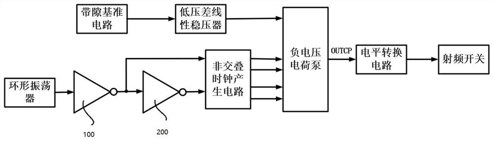
[0030]Embodiment 1: A control circuit applied to a low power supply voltage radio frequency switch: including a ring oscillator, a first inverter, a second inverter, a first non-overlapping clock generation circuit, and a second non-overlapping clock generation circuit Circuit, positive voltage charge pump, negative voltage charge pump, first level conversion circuit and second level conversion circuit. Wherein the output terminal of the ring oscillator is connected with the input terminal of the second inverter through the first inverter, and the output terminals of the first inverter and the second inverter are connected with two of the first non-overlapping clock generation circuit The input terminals are connected, the two output terminals of the first non-overlapping clock generating circuit are connected with the two input terminals of the positive voltage charge pump, the four output terminals of the positive voltage charge pump are respectively connected with the first ...

Embodiment 2

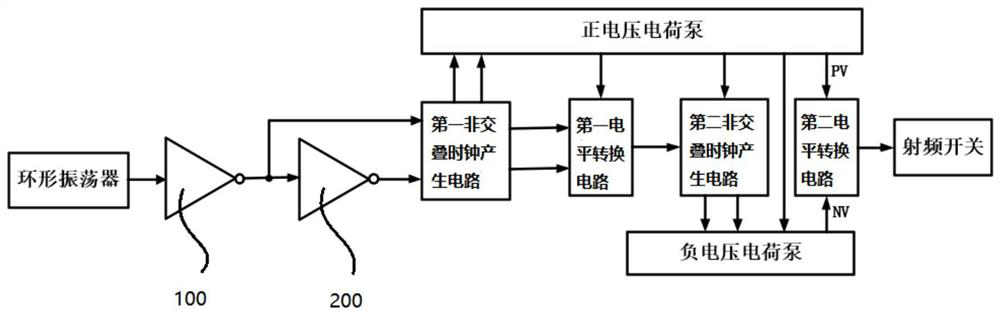
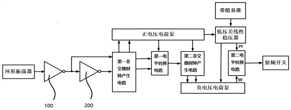
[0031] Embodiment 2: As a further preferred implementation, it includes a ring oscillator, a first inverter, a second inverter, a first non-overlapping clock generation circuit, a second non-overlapping clock generation circuit, and a positive voltage charge pump , Negative voltage charge pump, first level conversion circuit, second level conversion circuit, bandgap reference and low dropout linear regulator. Wherein the output end of the ring oscillator is connected to the input end of the inverter I2 via the inverter I1, and the output ends of the first inverter and the second inverter are connected to the two input ends of the first non-overlapping clock generation circuit The two output terminals of the first non-overlapping clock generation circuit are connected to the two input terminals of the positive voltage charge pump, and the three output terminals of the positive voltage charge pump are respectively connected to the first level conversion circuit and the second non...


PUM


Abstract

The invention discloses a control circuit applied to a low power supply voltage radio frequency switch, which comprises an annular oscillator, a first phase inverter, a second phase inverter, a first non-overlapping clock generation circuit, a second non-overlapping clock generation circuit, a positive voltage charge pump, a negative voltage charge pump, a first level conversion circuit and a second level conversion circuit, wherein three output ends of the positive voltage charge pump are respectively connected with the input ends of the first level conversion circuit, the second non-overlapping clock generation circuit and the negative voltage charge pump to be used as a power supply; the invention further discloses another structure, the structure further comprises a band-gap reference and a low dropout regulator, and three output ends of a positive voltage charge pump of the structure are respectively connected with input ends of the first level conversion circuit, the second non-overlapping clock generation circuit and the low dropout regulator to be used as a power supply. According to the structure, the circuit can be driven at a low level, the radio frequency switch can be controlled, and good radio frequency performance can still be kept when power is supplied by a low power source.

Description

technical field [0001] The invention belongs to the field of integrated circuits, in particular to a control circuit applied to low power supply voltage radio frequency switches. Background technique [0002] In a wireless communication transceiver, a high-performance switch is used for signal selection of the transmission path and the reception path, and its insertion loss, power capacity and other performances directly restrict the output power and noise figure performance of the entire system. Positive voltage generators above the supply voltage and negative voltage generators below ground are widely used to increase the dynamic range of handling power, enable efficient switching under DC bias conditions, and reduce quiescent current in the off-state. [0003] Because the charge pump power supply chip is small in size and high in efficiency, it is widely used in the market at present. The charge pump circuit uses the clock pulse to control the switch array to control the...

Claims


Application Information

Patent Timeline
Patent Type & Authority Applications(China)
IPC IPC(8): G05B19/042
CPCG05B19/0423G05B2219/25257
Inventor 刘小妮刘斌章国豪刘祖华陈哲
Owner 广州穗源微电子科技有限公司
Why Eureka
Try Eureka