Simulation method and system of LC-VCO (Inductance Capacitance-Voltage Controlled Oscillator)
A technology of LC-VCO and simulation method, applied in instrumentation, calculation, electrical digital data processing, etc., can solve problems such as large phase noise and affect design accuracy, and achieve the effect of improving phase noise
- Summary
- Abstract
- Description
- Claims
- Application Information
AI Technical Summary
Problems solved by technology
Method used
Image

Examples
Embodiment 1
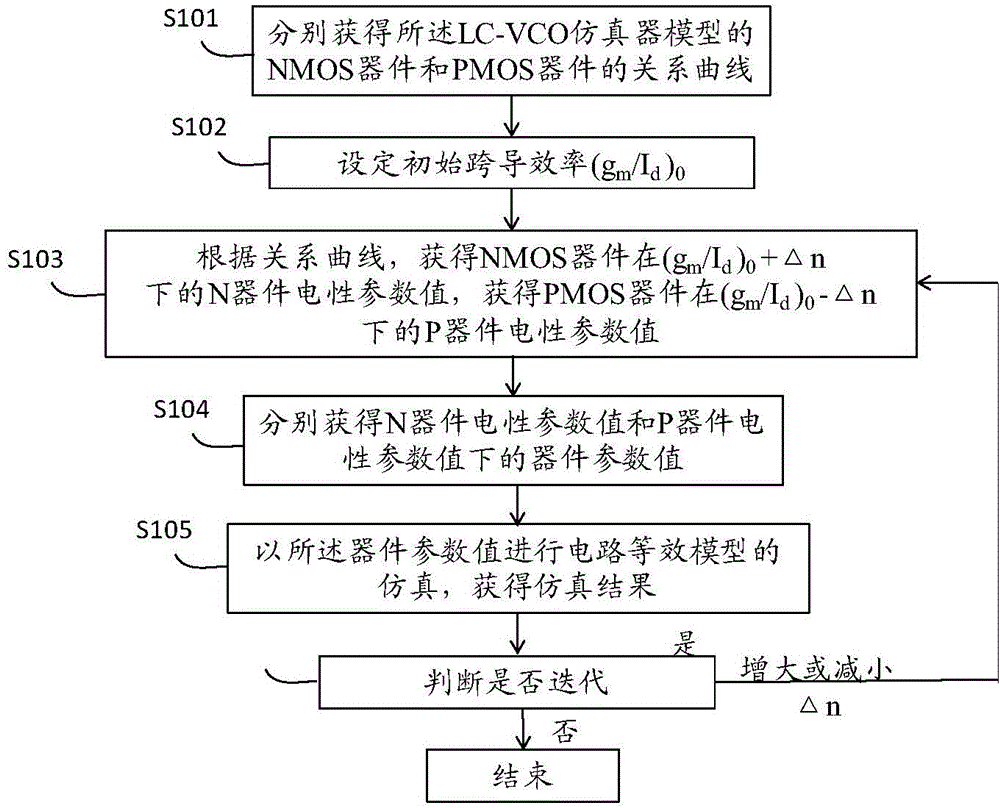
[0061] In this embodiment, the NMOS device and the PMOS device are respectively (g m / I D ) n and (g m / I D ) p The following parameters are simulated, and the simulation results are judged by the device simulation performance parameter values to improve the phase noise at the low frequency offset.
[0062] In step S103, keep I d unchanged, for NMOS devices, according to the relationship curve, the NMOS devices are obtained in (g m / I d ) n Under N device electrical parameter value, (g m / I d ) n =(g m / I d ) 0 +△n; for PMOS devices, according to the relationship curve, the PMOS device is obtained in (g m / I d ) p Under the P device electrical parameter value, (g m / I d ) p =(g m / I d ) 0 -△n, △n is the variation of transconductance efficiency.
[0063] In this step, it is carried out under the condition that the power consumption of the device remains unchanged, that is, the leakage current I of the device is kept d remain unchanged, and keep the osc...
Embodiment 2
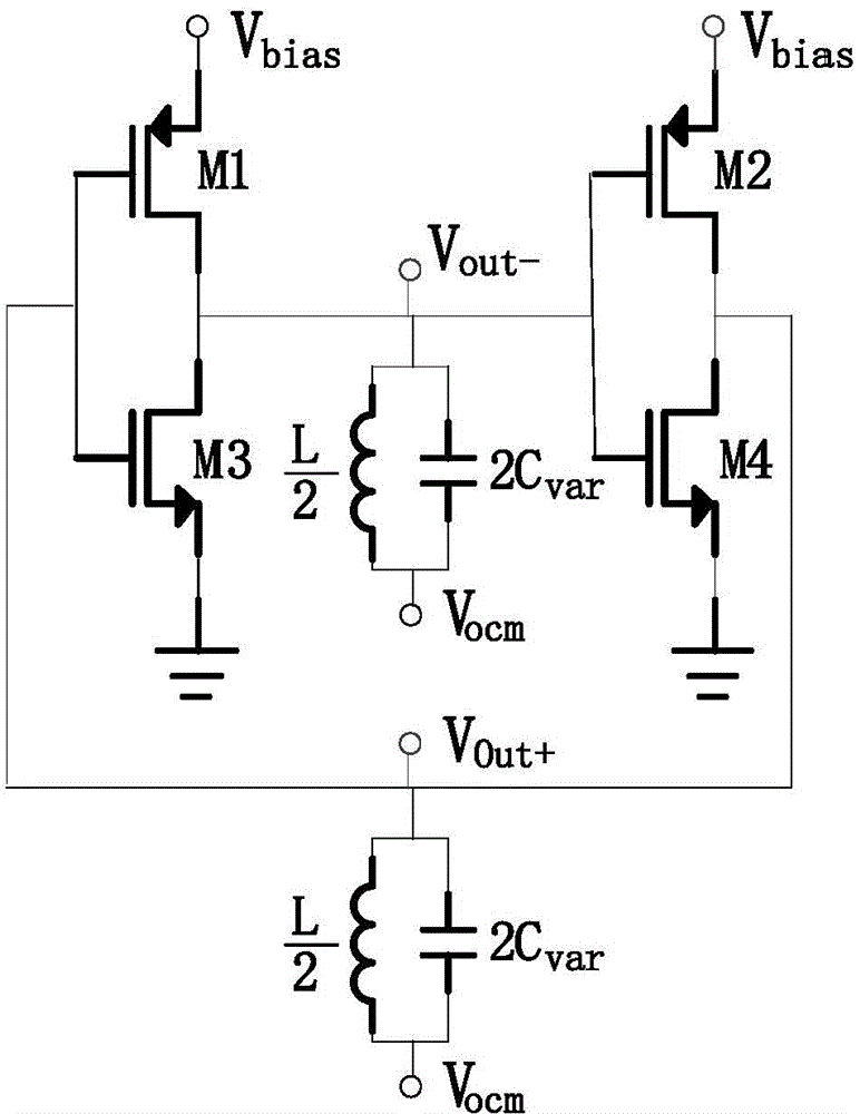
[0077] In this embodiment, the NMOS device and the PMOS device are respectively (g m / I D ) n and (g m / I D ) p The following parameters are simulated, and the simulation results are judged by the cut-off frequency or threshold voltage after oscillation, and the phase noise at the low frequency offset is improved.
[0078] Such as image 3 As shown, it is a schematic structural diagram of an analysis model of an LC-VCO according to an embodiment of the present invention. In this analysis model, the source terminals of the first PMOS device M1 and the second PMOS device M2 are connected to a DC bias voltage, and the first PMOS device M1 It forms an inverter with the first NMOS device M3, and the second PMOS device M2 and the second NMOS device M4 form an inverter. These two inverters are connected end to end to form a ring structure. At the same time, based on the analysis structure of the AC small signal, The resonant cavity of the inductance and capacitance is split int...
PUM
 Abstract
Description
Claims
Application Information
 - R&D
- Intellectual Property
- Life Sciences
- Materials
- Tech Scout
- Unparalleled Data Quality
- Higher Quality Content
- 60% Fewer Hallucinations
Browse by: Latest US Patents, China's latest patents, Technical Efficacy Thesaurus, Application Domain, Technology Topic, Popular Technical Reports.
© 2025 PatSnap. All rights reserved.Legal|Privacy policy|Modern Slavery Act Transparency Statement|Sitemap|About US| Contact US: help@patsnap.com