Polysilicon etching cavity and method capable of lowering metal pollutant content in cavity

A technology of polysilicon and etching chamber, which is applied in the field of microelectronics, can solve the problems of affecting the electrical performance of products, metal pollution of etching chamber 10, etc., and achieve the effect of improving product yield, reducing inherent damage, and reducing metal pollution content

Inactive Publication Date: 2016-12-07
SHANGHAI HUALI MICROELECTRONICS CORP
View PDF14 Cites 6 Cited by
  • Summary
  • Abstract
  • Description
  • Claims
  • Application Information

AI Technical Summary

Problems solved by technology

When the metal nail 16 is bombarded, it will excite a large amount of metal active ions and distribute them inside the etching chamber 10, causing the problem of metal pollution to the etching chamber 10.
Moreover, these metal active ions will be injected into the silicon wafer 15 under the action of strong pressure and strong current during the process, thus greatly affecting the electrical properties of the product

Method used


Image

  • Polysilicon etching cavity and method capable of lowering metal pollutant content in cavity
  • Polysilicon etching cavity and method capable of lowering metal pollutant content in cavity
  • Polysilicon etching cavity and method capable of lowering metal pollutant content in cavity

Examples


Embodiment Construction

[0026] The specific embodiment of the present invention will be further described in detail below in conjunction with the accompanying drawings.

[0027] It should be noted that, in the following specific embodiments, when describing the embodiments of the present invention in detail, in order to clearly show the structure of the present invention for the convenience of description, the structures in the drawings are not drawn according to the general scale, and are drawn Partial magnification, deformation and simplification are included, therefore, it should be avoided to be interpreted as a limitation of the present invention.

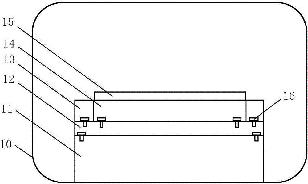
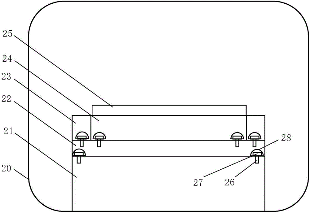
[0028] In the following specific embodiments of the present invention, please refer to figure 2 , figure 2 It is a schematic diagram of the structure of a polysilicon etching chamber for reducing metal pollution content in the chamber according to a preferred embodiment of the present invention. like figure 2 As shown, a polysilicon etching cha...


PUM


Abstract

The invention discloses a polysilicon etching cavity and a method capable of lowering metal pollutant content in the cavity. A plasma isolation apparatus is arranged on the exterior of an exposed top assembling structure of metal nails, wherein the metal nails are used for tightly locking a static adsorption plate, a lower electrode, a focus ring and a base; the metal nails are fully protected, so that the problem that the metal nails are subjected to etching plasma bombardment to generate metal active ions to cause metal pollution to the etching cavity in the cavity process period can be avoided completely; and an effect of lowering the metal pollutant content in the polysilicon etching cavity is achieved, thereby lowering inherent damage to the electrical performance of the product in the polysilicon etching process, and improving the product yield.

Description

technical field [0001] The invention relates to the field of microelectronics, in particular to a polysilicon etching chamber and method capable of reducing metal pollution content in the chamber. Background technique [0002] see figure 1 , figure 1 It is a schematic diagram of the internal structure of an existing polysilicon etching chamber. like figure 1 As shown, the polysilicon etching chamber 10 is provided with an electrostatic adsorption plate 14 for absorbing and fixing the silicon wafer 15 on the surface of the electrostatic adsorption plate 14 for processing. A lower electrode 12 is provided below the electrostatic adsorption disk 14 , a base 11 is provided below the lower electrode 12 , and a focus ring 13 is provided around the electrostatic adsorption disk 14 for protecting the lower electrode 12 below it. [0003] read on figure 1 . In the design of the electrostatic adsorption disc of the existing polysilicon etching machine, the nails 16 used to lock ...

Claims


Application Information

Patent Timeline
Patent Type & Authority Applications(China)
IPC IPC(8): H01L21/67H01J37/32
CPCH01J37/32458H01J37/32798H01L21/67069
Inventor 唐在峰许进任昱吕煜坤
Owner SHANGHAI HUALI MICROELECTRONICS CORP
Why Eureka
Try Eureka