Method for improving back stress of IGBT

A stress and organic adhesive technology, used in electrical components, semiconductor/solid-state device manufacturing, circuits, etc., can solve problems such as easy cracking of silicon wafers, and achieve the effect of reducing stress, improving stress, and improving cracking problems

Inactive Publication Date: 2016-12-07
SHANGHAI HUAHONG GRACE SEMICON MFG CORP
View PDF6 Cites 2 Cited by
  • Summary
  • Abstract
  • Description
  • Claims
  • Application Information

AI Technical Summary

Problems solved by technology

[0005] The technical problem to be solved by the present invention is to provide a method for improving...

Method used


Image

  • Method for improving back stress of IGBT
  • Method for improving back stress of IGBT
  • Method for improving back stress of IGBT

Examples


Embodiment Construction

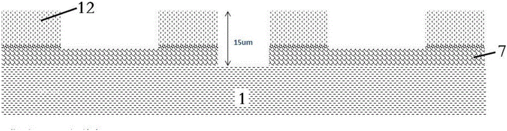
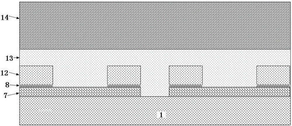
[0028] The method for improving IGBT stress described in the present invention, such as image 3 As shown, for the polyimide 12 covered on the passivation layer on the front side of the silicon wafer, after photolithography and etching patterning, an organic adhesive 13 is coated on the entire surface of the silicon wafer, and then a glass slide 14 is attached. The organic adhesive 13 is fully filled into the depressions and gaps after polyimide etching and patterning, and the glass slide 14 and the organic adhesive 13 together form a stress buffer layer.

[0029] The method for improving the back stress of the IGBT according to the present invention comprises the steps of:

[0030] In the first step, an organic adhesive with a thickness of 10-15 μm is spin-coated on a glass slide.

[0031] In the second step, an organic adhesive with a thickness of 10-15 μm is also coated on the front side of the silicon wafer.

[0032] In step 3, the front side of the silicon wafer is alig...


PUM

PropertyMeasurementUnit
Thicknessaaaaaaaaaa

Abstract

The invention discloses a method for improving back stress of an IGBT. Photoetching and etching patterning are carried out on polyimide covering a front passivation layer of a silicon wafer; the surface of the overall silicon wafer is coated with an adhesive; and then a glass slide is bonded. Recesses and gaps formed after polyimide etching are fully filled with the adhesive; and the glass slide and the adhesive form a stress buffer layer.

Description

technical field [0001] The invention relates to the field of design and manufacture of integrated circuits, in particular to a method for improving the back stress of an IGBT. Background technique [0002] IGBT (Insulated Gate Bipolar Transistor) Insulated Gate Bipolar Transistor is a composite fully-controlled voltage-driven power semiconductor device composed of BJT (Bipolar Transistor) and MOS (Insulated Gate Field Effect Transistor). The advantages of high input impedance and low conduction voltage drop of GTR. It is very suitable for the conversion system with a DC voltage of 600V and above, such as AC motors, frequency converters, switching power supplies, lighting circuits, traction drives and other fields. [0003] Common IGBT structures such as figure 1 As shown, the front side of substrate 1, namely figure 1 The upper part is the gate 2 on the front of the IGBT, the gate oxide layer 3, the P well 4, the front metal connection 7 and so on. the back, ie figure 1...

Claims


Application Information

Patent Timeline
IPC IPC(8): H01L21/683
CPCH01L21/6835
Inventor 马彪黄璇
Owner SHANGHAI HUAHONG GRACE SEMICON MFG CORP
Why Eureka
Try Eureka