Quad flat non-leaded package structure and leadframe thereof

A leadless packaging, square flat technology, used in semiconductor devices, semiconductor/solid-state device parts, electrical components, etc. problems such as abnormal sexual connection, to achieve the effect of improving yield and simplifying processing complexity

Inactive Publication Date: 2016-12-07
CHIPMOS TECH INC
View PDF7 Cites 1 Cited by
  • Summary
  • Abstract
  • Description
  • Claims
  • Application Information

AI Technical Summary

Problems solved by technology

[0003] However, after the bonding process between the chip and the lead frame is completed, it is usually necessary to remove the above-mentioned back adhesive film for subsequent processing, and the removal of the back adhesive film requires additional processing, which usually increases the manufacturing cost and man-hours.
In addition, removing the adhesive film after the chip is electrically connected to the lead frame may cause the lead frame, bonding wires, and bumps to be pulled, resulting in an abnormal situation in the electrical connection between the chip and the lead frame, which has the potential to reduce the packaging yield. possible

Method used


Image

  • Quad flat non-leaded package structure and leadframe thereof
  • Quad flat non-leaded package structure and leadframe thereof
  • Quad flat non-leaded package structure and leadframe thereof

Examples


Embodiment Construction

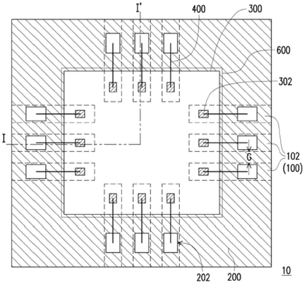
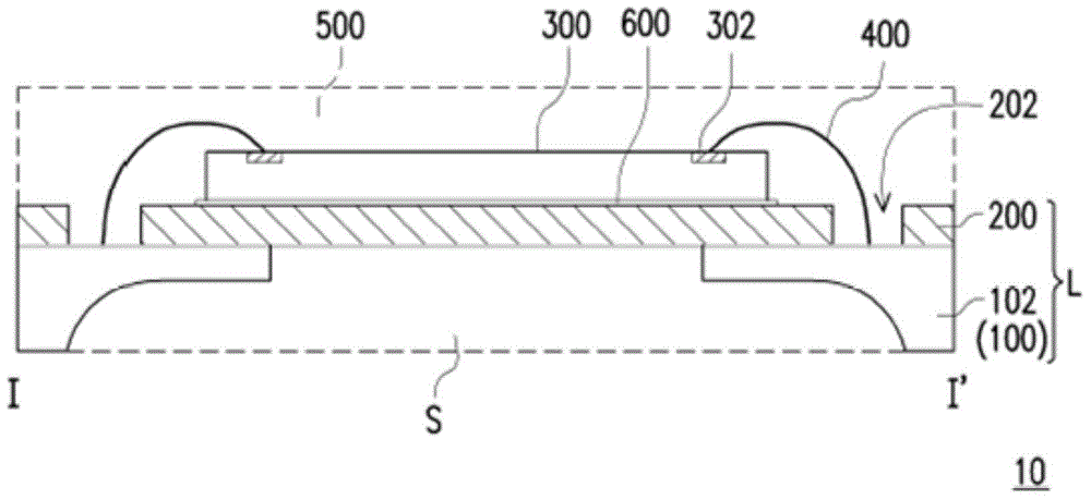
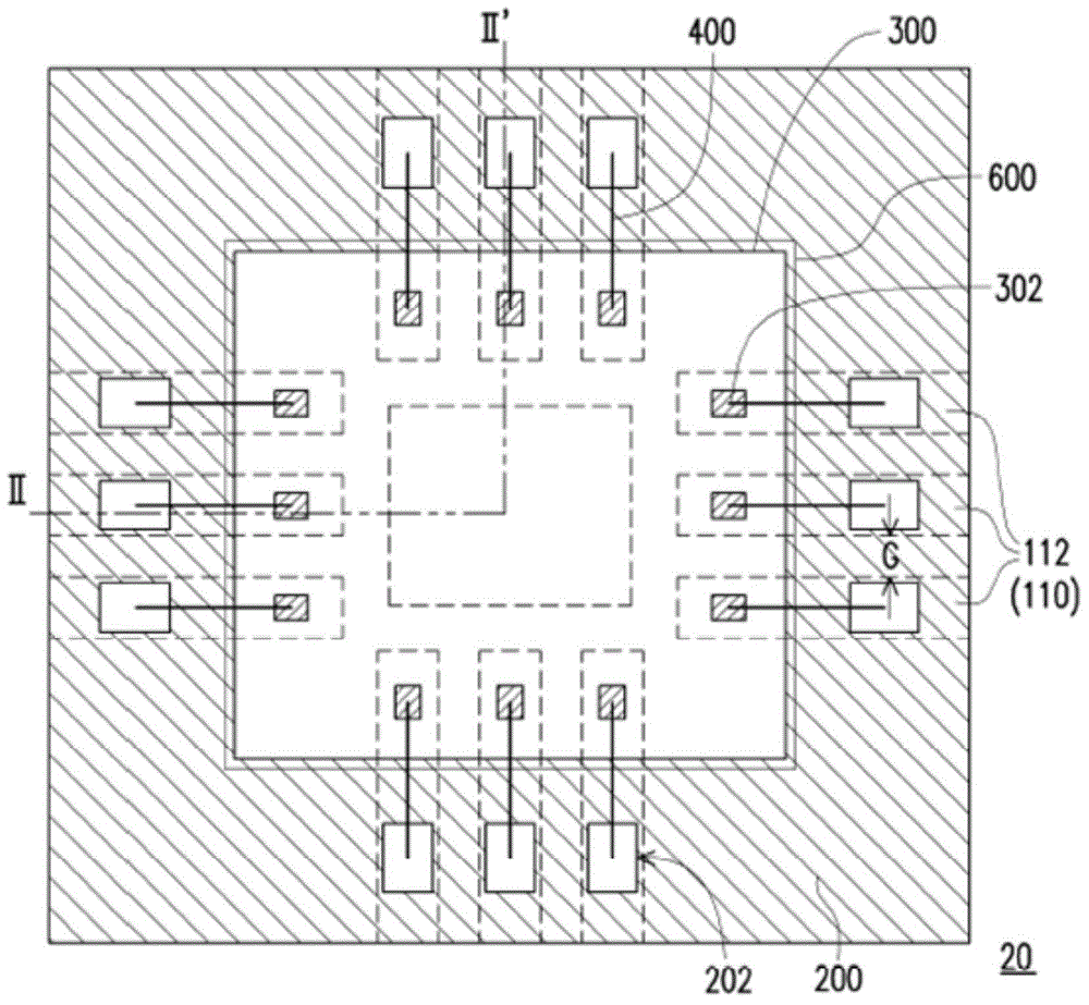
[0044] Figure 1A It is a top view of a quad flat no-lead package structure according to an embodiment of the present invention. Figure 1B for Figure 1A The cross-sectional schematic diagram of the quadflat no-lead package structure along the section line I-I'. Please also refer to Figure 1A and Figure 1B , in this embodiment, the QFN package structure 10 includes a lead frame 100 , a dielectric film 200 , a chip 300 , a plurality of bonding wires 400 and an encapsulant 500 . To clearly illustrate the present invention, the distribution range of the encapsulant 500 will be indicated by a dotted line, and the dielectric film 200 will be indicated by an oblique line. For the convenience of explanation below, the lead frame 100 drawn in the drawings of the present invention is only one of the units on the entire lead frame. In practice, the dielectric film 200 is a thin film formed corresponding to the size of the entire lead frame. In order to fully cover each unit of the ...


PUM


Abstract

A quad flat non-leaded package structure including a leadframe, a dielectric layer, a chip, a plurality of bonding wires and a molding compound is provided. The leadframe includes a plurality of leads. The dielectric layer disposed on the leadframe. The dielectric layer has a plurality of openings. Each opening is located on the corresponding lead respectively. The chip is disposed on the dielectric layer. Each bonding wire is connected between the chip and the lead exposed corresponding the opening. The molding compound encapsulates the leadframe, the dielectric layer, the chip and the bonding wires. A leadframe for a quad flat non-leaded flip chip leadframe package is also provided. The quad flat non-leaded package structure simplifies the processing complexity and improves the yield.

Description

technical field [0001] The invention relates to a semiconductor package structure, in particular to a square flat leadless package structure and a lead frame structure. Background technique [0002] Semiconductor packaging technology includes many packaging forms, among which the quad flat no-lead package of the quad flat package series has a short signal transmission path and a relatively fast signal transmission speed, so it is one of the mainstream packaging forms. Generally speaking, when the chip is bonded to the lead frame, such as wire bonding or flip chip bonding, a backside tape must be provided on the bottom of the lead frame to allow the wire The position of the frame can be fixed by vacuum suction, so as to ensure the smooth progress of the wire bonding or flip-chip bonding process, thereby improving the yield rate of the bonding process between the chip and the lead frame. [0003] However, after the bonding process between the chip and the lead frame is comple...

Claims


Application Information

Patent Timeline
Patent Type & Authority Applications(China)
IPC IPC(8): H01L23/31H01L23/495
CPCH01L2224/16245H01L2224/48091H01L2224/49175H01L2224/73265H01L2924/00014
Inventor 吴自胜
Owner CHIPMOS TECH INC
Why Eureka
Try Eureka