Image sensor module and manufacturing method thereof

A technology of image sensor and manufacturing method, applied in the sensor field

Inactive Publication Date: 2016-12-07
苏州科阳半导体有限公司
View PDF5 Cites 35 Cited by
  • Summary
  • Abstract
  • Description
  • Claims
  • Application Information

AI Technical Summary

Problems solved by technology

[0005] In view of this, the present invention proposes an image sensor module and its manufacturing method to solve the problems...

Method used


Image

  • Image sensor module and manufacturing method thereof
  • Image sensor module and manufacturing method thereof
  • Image sensor module and manufacturing method thereof

Examples


Embodiment 1

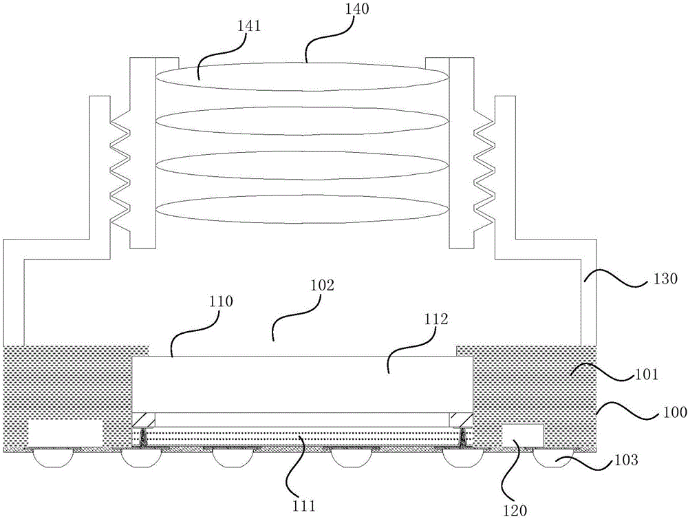
[0051] figure 1 It is a schematic structural diagram of the image sensor module provided by Embodiment 1 of the present invention. The image sensor module provided by the embodiments of the present invention can be applied to electronic devices such as smart phones, tablet computers, digital cameras, car driving recorders, and children's toys.

[0052] Such as figure 1 As shown, the image sensor module provided in this embodiment includes:

[0053] The image sensing chip 110 and at least one auxiliary chip 120, the image sensing chip 110 and at least one auxiliary chip 120 are packaged into a chip package 100 by the plastic packaging material 101, and the circuit of the image sensing chip 110 and at least one auxiliary chip 120 face in the same direction;

[0054] The image sensing chip 110 includes an image sensing unit 111, and an encapsulation glass 112 arranged above the light-incident surface of the image sensing unit 111. The front side of the above-mentioned chip pac...

Embodiment 2

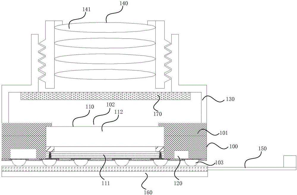
[0064] figure 2 It is a schematic structural diagram of the image sensor module provided by Embodiment 2 of the present invention. Such as figure 2 As shown, further, the image sensor module provided in this embodiment also includes a rigid-flex board 150 , wherein the rigid-flex board 150 includes a conductive circuit layer, and a plurality of solder joints arranged on the front surface of the rigid-flex board 150 The multiple pads are respectively electrically connected to the multiple bumps 103 on the redistribution pattern on the back of the chip package 100 .

[0065] Rigid-flex boards, that is, flexible circuit boards (FPC) and rigid circuit boards (PCB), are combined according to relevant process requirements after lamination and other processes to form circuit boards with FPC characteristics and PCB characteristics. The image sensor module provided by Embodiment 2 of the present invention is attached to the rigid-flex board 150. The rigid-flex board 150 has both a ...

Embodiment 3

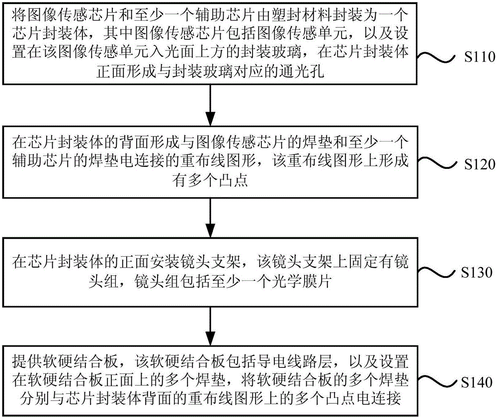
[0074] image 3 It is a flow chart of the manufacturing method of the image sensor module provided by the third embodiment of the present invention. This embodiment provides a method for manufacturing an image sensor module, including:

[0075] S110, packaging the image sensing chip and at least one auxiliary chip into a chip package with a plastic packaging material, wherein the image sensing chip includes an image sensing unit, and packaging glass arranged above the light-incident surface of the image sensing unit, A light hole corresponding to the packaging glass is formed on the front of the chip package;

[0076] S120, forming a rewiring pattern electrically connected to the bonding pad of the image sensor chip and the bonding pad of at least one auxiliary chip on the back of the chip package, and a plurality of bumps are formed on the rewiring pattern;

[0077] S130. Install a lens holder on the front surface of the chip package, a lens group is fixed on the lens holde...


PUM


Abstract

The embodiment of the invention discloses an image sensor module which comprises an image sensing chip, at least one auxiliary chip and a lens bracket. The image sensing chip and at least one auxiliary chip are packaged by a plastic package material to form a chip package body, the circuit faces of the image sensing chip and at least one auxiliary chip face the same direction. The image sensing chip comprises an image sensing unit and package glass arranged above the incident face of the image sensing unit, a light through hole corresponding to the package glass is formed in the front side of the chip package body, a wire re-arrangement graph electrically connected with the welding pad of the image sensing chip and the welding pads of at least one auxiliary chip is formed on the back side of the chip package body, and multiple convex points are formed on the wire re-arrangement graph. The lens bracket is installed on the front side of the chip package body, and a lens group is fixed to the lens bracket. The reliability of the image sensor module is improved, and the wire arrangement difficulty is reduced.

Description

technical field [0001] The invention relates to the field of sensors, in particular to an image sensor module and a manufacturing method thereof. Background technique [0002] An image sensor chip is a semiconductor device that senses external light and converts it into electrical signals. After the image sensor chip is manufactured, a series of packaging processes are first performed on the image sensor chip, and then the mirror mount bracket and the lens are installed to form an image sensor module. Image sensor modules are mainly used in electronic devices such as smartphones, tablet computers, digital cameras, car driving recorders, and children's toys. [0003] The existing image sensor chip packaging method is mainly COB (Chip On Board) packaging, the bare chip is attached to the interconnection substrate with conductive or non-conductive adhesive, and then wire bonding is performed to realize its electrical connection. The image sensor packaging method in the prior ...

Claims


Application Information

Patent Timeline
IPC IPC(8): H01L23/31H01L27/146
CPCH01L27/146H01L23/3114
Inventor 朱文辉吕军王邦旭赖芳奇
Owner 苏州科阳半导体有限公司
Why Eureka
Try Eureka