Manufacturing method of HDI circuit board

A production method and circuit board technology, which are applied in multilayer circuit manufacturing, printed circuit manufacturing, printed circuit and other directions, can solve the problems of large knife wear and long working hours, and achieve the effect of reducing production cost and shortening production period.

Inactive Publication Date: 2016-12-07
JIANGSU BOMIN ELECTRONICS
View PDF6 Cites 8 Cited by
  • Summary
  • Abstract
  • Description
  • Claims
  • Application Information

AI Technical Summary

Problems solved by technology

[0004] However, the drilling of target holes requires the use of special X-RAY drilling equipment, which consumes

Method used


Image

  • Manufacturing method of HDI circuit board
  • Manufacturing method of HDI circuit board
  • Manufacturing method of HDI circuit board

Examples


Embodiment Construction

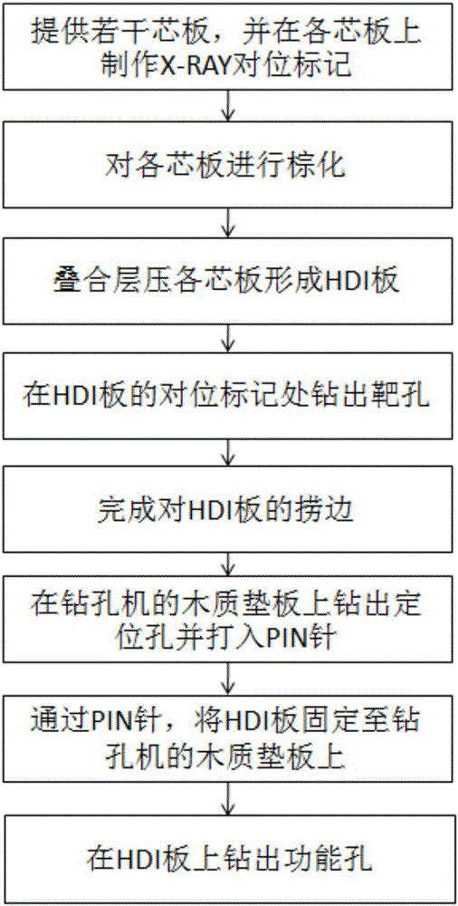
[0024] In order to make the above objects, features and advantages of the present invention more comprehensible, the present invention will be further described in detail below in conjunction with the accompanying drawings and specific embodiments.

[0025] Such as figure 2 , the manufacture method of a kind of HDI circuit board of the present invention, comprises the steps:

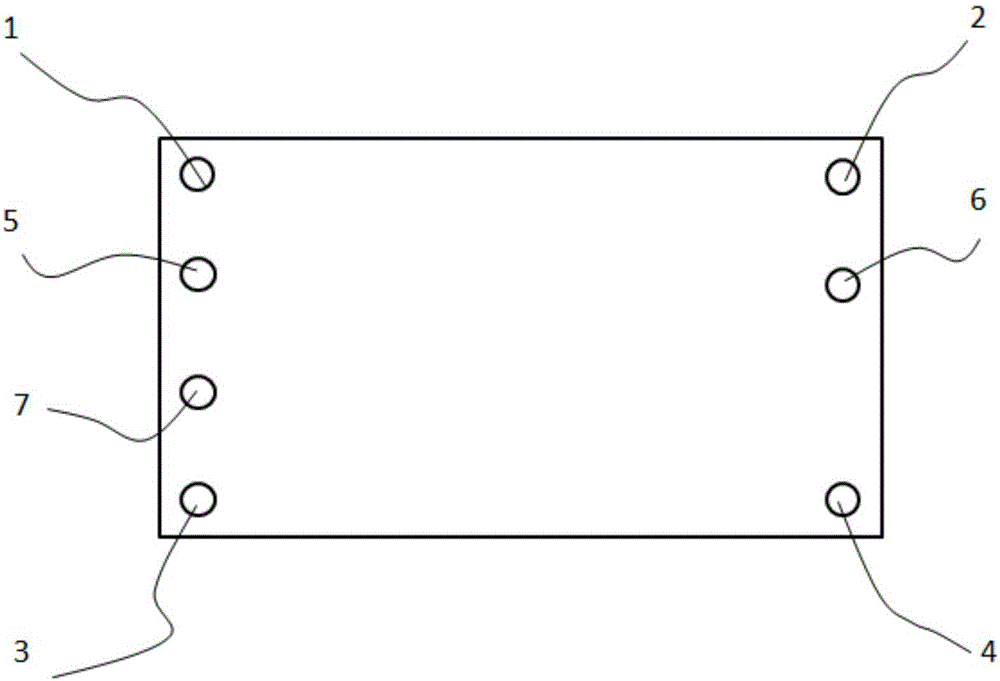
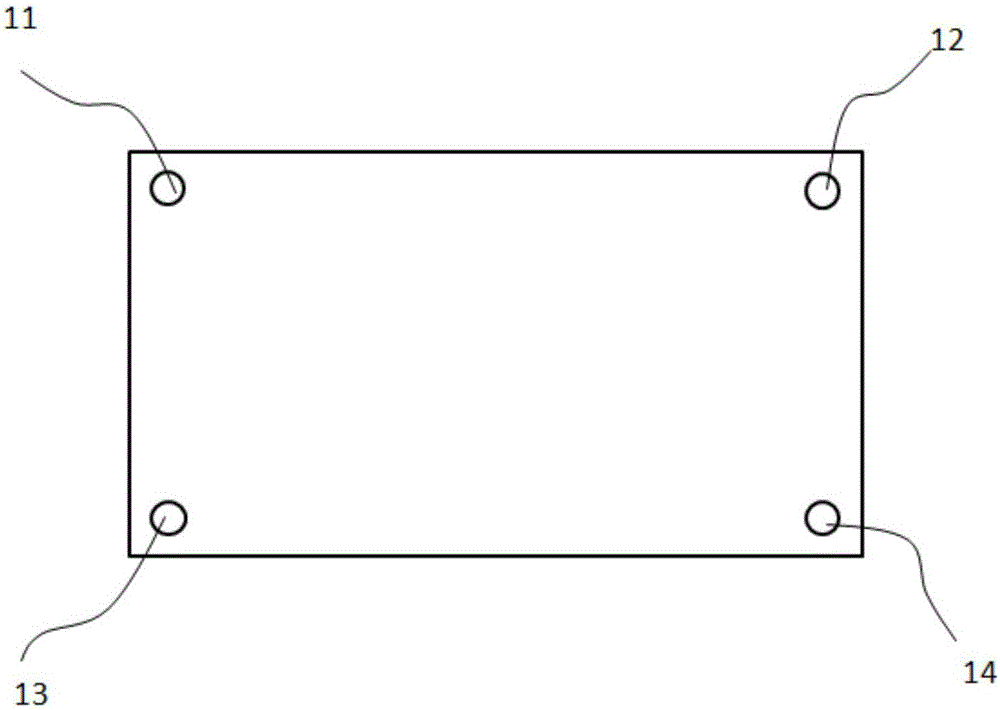
[0026] Step 1: Provide several core boards, and set X-RAY alignment marks on the upper surface of each core board. In this embodiment, each core board is a rectangular core board with copper foil on its surface, and the alignment marks are evenly distributed on the four corners of the core board.

[0027] Step 2: Browning each core board, that is, roughening the smooth copper foil layer on the upper and lower surfaces of the core board, so as to enhance the bonding force of the core board in the subsequent lamination and lamination process.

[0028] Step 3: The core boards are stacked and laminated in...


PUM

PropertyMeasurementUnit
Thicknessaaaaaaaaaa

Abstract

The invention discloses a manufacturing method of an HDI circuit board. The method comprises the following steps of (1) providing a plurality of core boards, and arranging X-RAY alignment marks at four corners of each core board; (2) sequentially superimposing and laminating the core boards to form the HDI circuit board; (3) drilling target holes which run through the HDI circuit board on the alignment marks by employing an X-RAY target drilling machine; (4) routing the HDI circuit board by using a routing machine; (5) drilling locating holes which are matched with the target holes for use in a wooden base plate of a drilling machine and driving a PIN needle into each locating hole; (6) fixing the HDI circuit board on the upper surface of the wooden base plate through the PIN needles; and (7) carrying out scanning and locating on the four target holes in the HDI circuit board through the drilling machine to determine the positions of function holes in the upper surface of the HDI circuit board and to drill the function holes. By the manufacturing method of the HDI circuit board disclosed by the invention, subsequent routing, function hole drilling and laser processes can be achieved only by drilling the four target holes in the upper surface of the HDI circuit board, so that the production cost is effectively reduced and the production period is shortened.

Description

technical field [0001] The invention relates to the field of circuit board production, in particular to a method for producing an HDI circuit board. Background technique [0002] HDI circuit boards are also called high-density interconnection boards. The production process of HDI circuit boards includes sub-core board preparation, lamination and lamination, edge removal, functional hole drilling, laser and many other processes. Among them, edge fishing, functional hole drilling and laser technology all require precise positioning of HDI circuit boards, so X-RAY drilling equipment must be used to drill several target holes on HDI circuit boards to achieve precise positioning. [0003] see figure 1 , in the prior art, it is generally necessary to drill seven target holes on the HDI circuit board, which is the so-called seven-hole operation mode. The seven target holes are the first target hole 1, the second target hole 2, the third target hole 3 and the fourth target hole 4 ...

Claims


Application Information

Patent Timeline
IPC IPC(8): H05K3/46
CPCH05K3/4638H05K2203/166
Inventor 黄继茂傅廷昌李佳卞爱明金敏王瑜
Owner JIANGSU BOMIN ELECTRONICS
Why Eureka
Try Eureka