Preparation method for high-density interconnection board

A technology of high-density interconnection board and manufacturing method, which is applied in the direction of multi-layer circuit manufacturing, printed circuit manufacturing, electrical components, etc. Bit accuracy and drilling accuracy of laser drilling stack holes, reducing the number of electroplating and grinding, and reducing the effect of production processes

Inactive Publication Date: 2016-12-07
JIANGMEN SUNTAK CIRCUIT TECH
View PDF4 Cites 8 Cited by
  • Summary
  • Abstract
  • Description
  • Claims
  • Application Information

AI Technical Summary

Problems solved by technology

[0013] The purpose of the present invention is to provide a method for manufacturing high-density interconnection boards, which aims to solve the technical problems in the prior art that the process of making high-density interconnection boards is lengthy and the quality of the produced products is prone to defects

Method used


Image

  • Preparation method for high-density interconnection board
  • Preparation method for high-density interconnection board
  • Preparation method for high-density interconnection board

Examples


Embodiment Construction

[0058] Embodiments of the present invention are described in detail below, examples of which are shown in the drawings, wherein the same or similar reference numerals designate the same or similar elements or elements having the same or similar functions throughout. Attached below by reference Figure 2-6 The described embodiments are exemplary and are intended to explain the present invention, but should not be construed as limiting the present invention.

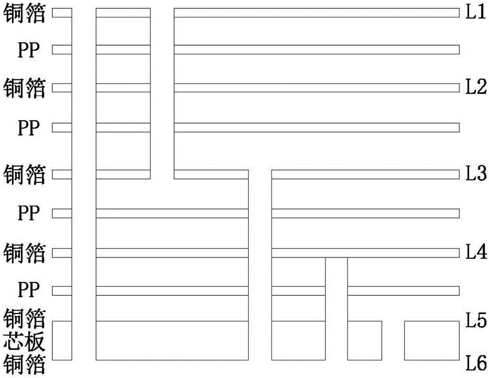
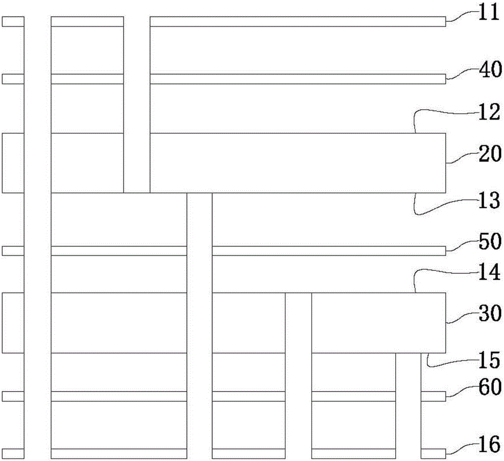
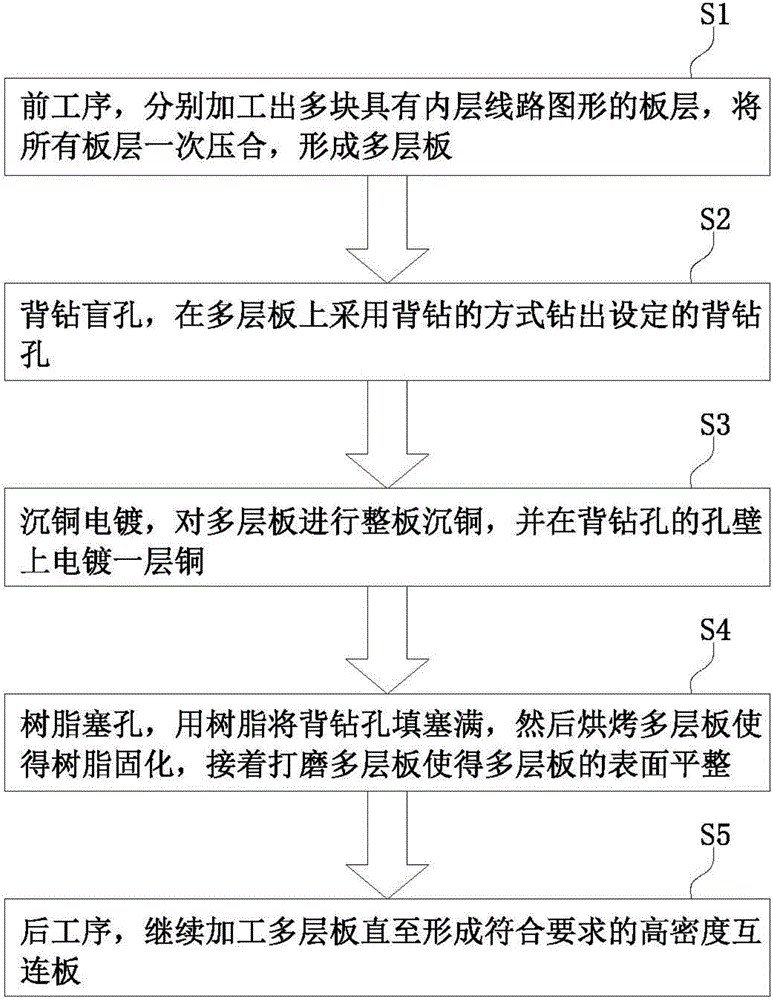
[0059] Such as Figure 2~3 As shown, a method for manufacturing a high-density interconnection board provided by an embodiment of the present invention includes the following steps:

[0060] S1: In the previous process, several layers with inner circuit patterns are processed separately, and all the layers are pressed together at one time to form a multi-layer board;

[0061] S2: back-drilling blind holes, drilling set back-drilling holes on the multi-layer board by means of back-drilling;

[0062] S3: Copper immersion ...


PUM


Abstract

The invention relates to the technical field of printed circuit board production and especially relates to a preparation method for a high-density interconnection board. The preparation method for the high-density interconnection board comprises the steps of carrying out a front process of processing multiple board layers with inner circuit patterns and laminating all board layers once, thereby forming a multilayer board; carrying out a blind hole back drill step of drilling a set back drill hole in a back drill mode; carrying out an electroless plating copper electroplating step of carrying out whole board electroless plating copper on the multilayer board and electroplating a layer of copper on the hole wall of the back drill hole; carrying out a resin hole plugging step of plugging the back drill hole by employing resin, baking the multilayer board, thereby enabling the resin to be cured, and then polishing the multilayer board, thereby enabling the surface of the multilayer board to be flat; and carrying out a post process of continuously processing the multilayer board until the high-density interconnection board satisfying a demand is formed. According to the method, multiple times of electroplating and copper reduction processes can be avoided, the copper thickness uniformity can be ensured, the electroplating and board polishing times can be reduced and the quality of the produced high-density interconnection board can be improved.

Description

technical field [0001] The invention relates to the technical field of manufacturing printed circuit boards, in particular to a method for manufacturing high-density interconnection boards. Background technique [0002] Existing high-density interconnection boards mostly use any layer interconnection, such as figure 1 As shown, in the production process, the L5-L6 layer blind holes are made first, and then the L4-L5 layer blind holes are made, and the blind holes of each layer are made in turn, and some blind holes need to be stacked blind holes, and the production process is lengthy; at the same time, the resin Abrasive belt grinding is required in the plugging process, which will affect the expansion and contraction of the high-density interconnection board after the abrasive belt grinding. Even the scrapping of the board. In addition, the outer layer (L6 layer) needs to be electroplated multiple times during the process of making blind holes and inner layer resin plug h...

Claims


Application Information

Patent Timeline
IPC IPC(8): H05K3/46
CPCH05K3/4614
Inventor 王文明孙玉凯王佐韩启龙付胜
Owner JIANGMEN SUNTAK CIRCUIT TECH
Why Eureka
Try Eureka