Circuit board

A technology of circuit boards and substrates, which is applied in the direction of printed circuits, printed circuits, circuit devices, etc., can solve the problems of signal integrity, large through-hole area of ​​the formation, discontinuous formation, etc., to ensure integrity, reliability, The effect of reducing the number

Inactive Publication Date: 2016-12-14
SHENZHEN TINNO WIRELESS TECH
View PDF6 Cites 3 Cited by
  • Summary
  • Abstract
  • Description
  • Claims
  • Application Information

AI Technical Summary

Problems solved by technology

[0003] However, the pins of the chip are relatively large and dense. If each pin transmits a signal through a through-hole, the number of through-holes needs to be opened is very large, resulting in too large a through-hole area in the formation, and the formation is discontinuous, resulting in signal integrity. When encountering ESD (Electro-Static discharge, electrostatic discharge) problems, static electricity cannot be released quickly, which will affect the normal operation of the system

Method used


Image

  • Circuit board
  • Circuit board
  • Circuit board

Examples


Embodiment Construction

[0036] The present application will be further described in detail below through specific embodiments in conjunction with the drawings. The "front", "rear", "left", "right", "up" and "down" mentioned in the text are all based on the placement state in the drawings.

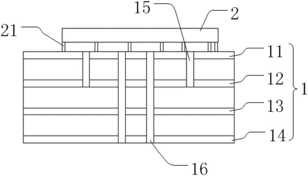
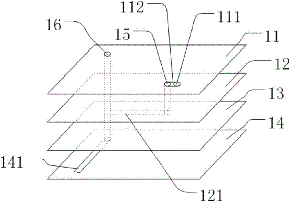
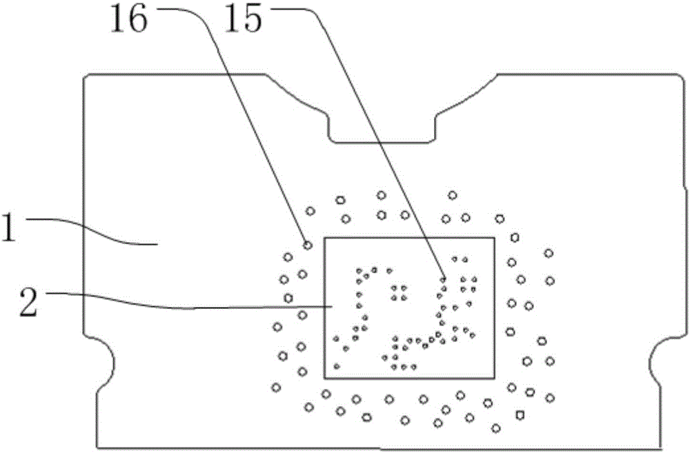
[0037] Such as Figure 1-3 As shown, the embodiment of the present application provides a circuit board including a substrate 1 and a first conductive member. The substrate 1 includes a device layer 11, a signal layer 12, and a ground layer 13, and the device layer 11, the signal layer 12, and the ground layer 13 are stacked, And the signal layer 12 is located between the device layer 11 and the ground layer 13, and the device layer 11 is provided with a plurality of pads 111; the substrate 1 is provided with a blind hole 15 which extends from the device layer 11 to the signal layer 12, that is, does not penetrate In the ground layer 13, the first conductive member is provided in the blind hole 15, that is, each bli...


PUM


Abstract

The invention relates to the technical field of circuit board production, in particular to a circuit board which comprises a substrate and first conductive parts. The substrate comprises a device layer, a signal layer and a ground layer which are arranged in an overlapped mode, the signal layer is located between the device layer and the ground layer, and the device layer is provided with multiple welding disks; the substrate is provided with blind holes which extend to the signal layer from the device layer, one first conductive part is arranged in each blind hole, and at least one welding disk is electrically conducted with the signal layer through the first conductive parts. According to the circuit board, the blind holes are arranged and each internally provided with one first conductive part, and the welding disks on the device layer can be electrically connected with the signal layer through the first conductive parts; therefore, the number of through holes in the circuit board can be decreased, destruction to the ground layer is reduced, the integrity of the ground layer is well guaranteed, when an ESD problem occurs, static electricity can be rapidly released, and the reliability of the system is guaranteed.

Description

Technical field [0001] This application relates to the technical field of circuit board production, in particular to a circuit board. Background technique [0002] In the production of multi-layer circuit boards, especially chips with denser pins, such as a circuit board including a CPU (Central Processing Unit, central processing unit), through holes are often opened to realize signal transmission, and the through holes penetrate through each layer, including In the ground layer, the through holes transmit the signal from the surface layer to the other layers. [0003] However, the pins of the chip are many and dense. If each pin transmits signals through through holes, the number of through holes that need to be opened is extremely large, resulting in too large through holes in the ground layer, discontinuous ground layer, and complete signal When encountering ESD (Electro-Static Discharge, electrostatic discharge) problems, static electricity cannot be quickly discharged, which...

Claims


Application Information

Patent Timeline
IPC IPC(8): H05K1/02H05K1/11
CPCH05K1/0259H05K1/116H05K2201/093
Inventor 罗鸿飞曾永聪
Owner SHENZHEN TINNO WIRELESS TECH
Why Eureka
Try Eureka