Touch panel and manufacturing method thereof

A technology of touch panel and touch electrode, which is applied in the direction of instruments, electrical digital data processing, and input/output process of data processing, etc., and can solve problems such as being easily scratched or oxidized

Pending Publication Date: 2017-01-04
ANHUI JINGZHUO OPTICAL DISPLAY TECH CO LTD
View PDF8 Cites 8 Cited by
  • Summary
  • Abstract
  • Description
  • Claims
  • Application Information

AI Technical Summary

Problems solved by technology

And some types of touch screens, such as OGS (OneGlass Solution, that is, integrated touch) touch screens, DITO (with two layers of ITO layers) touch screens, etc., the ITO conductive layer is exposed on the side facing away from the protective cover, which is easy to be scratched or damaged. oxidation

Method used


Image

  • Touch panel and manufacturing method thereof
  • Touch panel and manufacturing method thereof
  • Touch panel and manufacturing method thereof

Examples


Embodiment Construction

[0050] The touch panel and its manufacturing method will be further described below in conjunction with the accompanying drawings and specific embodiments.

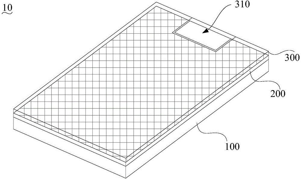
[0051] Such as figure 1 As shown, the touch panel 10 according to one embodiment includes a transparent substrate 100 , a conductive layer 200 and a first transparent photosensitive resin layer 300 .

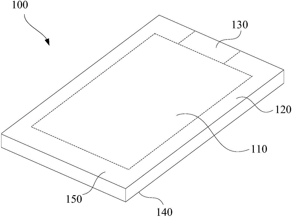
[0052] Such as figure 2 As shown, the transparent substrate 100 has a visible area 110 and a non-visible area 120, and the non-visible area 120 is provided with a binding area 130 for binding with a flexible circuit board.

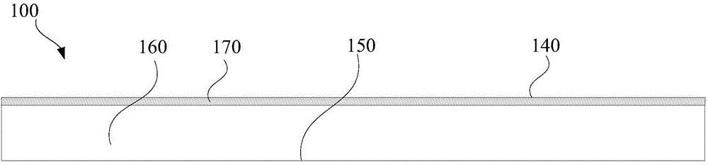
[0053] The touch panel 10 needs to have a protective cover. In this embodiment, the transparent substrate 100 is also the protective cover of the touch panel 10 . That is, the transparent substrate 100 has a touch surface 140 and a bearing surface 150 opposite to each other. Wherein, the surface hardness of the touch surface 140 is greater than or equal to 3H (3H is a pencil hardness level), so tha...


PUM


Abstract

The invention relates to a touch panel and a manufacturing method thereof. The touch panel comprises a transparent substrate, a conductive layer and a first transparent photosensitive resin layer, wherein the transparent substrate is provided with a visual area and a non-visual area, and the non-visual area is provided with a binding area used for being bound to a flexible circuit board; the conductive layer is arranged on one surface of the transparent substrate and comprises an electrode pattern and a lead, the electrode pattern is located on the visual area and used for obtaining coordinate information of a touch point, the lead is connected with the electrode pattern and used for transmitting the coordinate information obtained by the electrode pattern through the flexible circuit board, the end, connected with the electrode pattern, of the lead serves as a first end, and the other end of the lead serves as a second end and is located in the binding area; the first transparent photosensitive resin layer is disposed on the surface, away from the transparent substrate, of the conductive layer, and the first transparent photosensitive resin layer is concave from the edge of the transparent substrate to form a notch so that the second end can be exposed. The touch panel can effectively protect the conductive layer and prevent the conductive layer from being scratched or oxidized.

Description

technical field [0001] The invention relates to the field of touch technology, in particular to a touch panel and a manufacturing method thereof. Background technique [0002] As an inductive device that can accept touch input signals, the touch screen has increasingly replaced the traditional mechanical keyboard input, and is widely used in consumer electronics such as smartphones, tablet computers, and notebook computers, as well as electronic blackboards and vending machines. Where human-computer interaction is required. [0003] Traditional touch screens usually use indium tin oxide (ITO) as the conductive layer material. Specifically, when making a touch screen, the ITO conductive layer is first formed by magnetron sputtering, and then the ITO conductive layer is processed by etching to make a transparent electrode pattern, wherein the transparent electrode pattern is used to determine the coordinates of the touch point information. [0004] In practical applications...

Claims


Application Information

Patent Timeline
Patent Type & Authority Applications(China)
IPC IPC(8): G06F3/041G06F3/044
Inventor 胡丽叶剑
Owner ANHUI JINGZHUO OPTICAL DISPLAY TECH CO LTD
Why Eureka
Try Eureka