

Inductive coupling plasma processing system and processing method
A technology for processing systems and plasmas, applied to plasmas, circuits, discharge tubes, etc., can solve the problems of certain reflected power, inability to match, and affect the shape of through holes, etc., to achieve wide impedance matching range, fast and accurate impedance, The effect of improving the shape
- Summary
- Abstract
- Description
- Claims
- Application Information
AI Technical Summary
Problems solved by technology
Method used
Image

Examples
Embodiment Construction
[0025] In order to make the purpose, technical solution, and beneficial effects of the present invention clearer and more complete, the following describes specific implementations of the present invention in conjunction with the accompanying drawings.
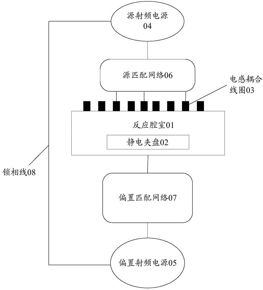
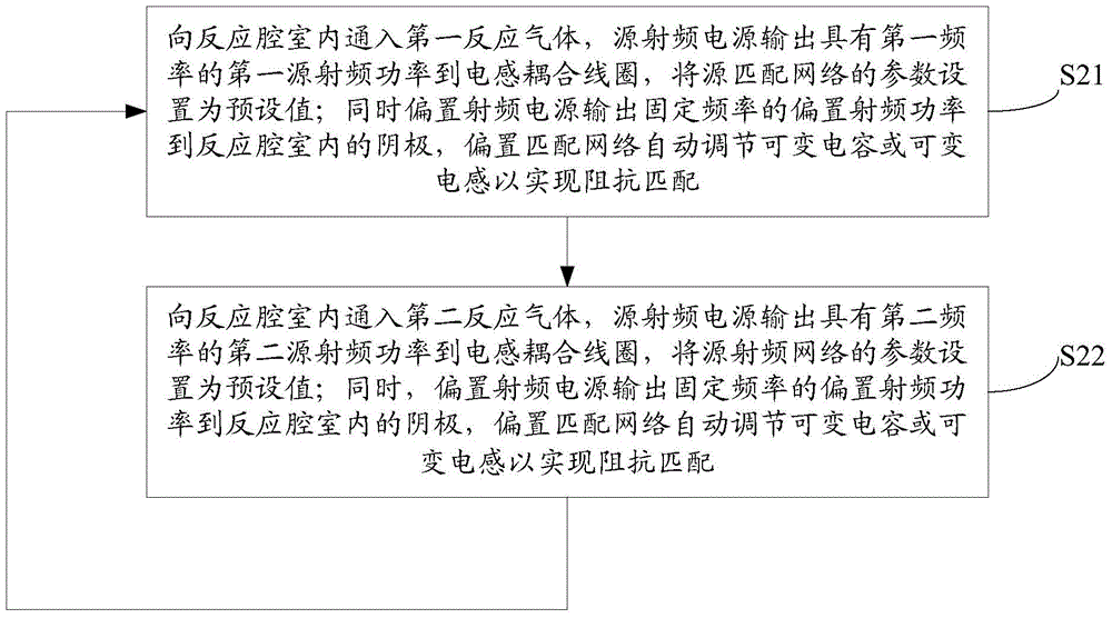
[0026] As mentioned in the background technology section, either there is a defect of slow response speed in the existing matching network, or the small reflected power cannot be obtained all the time under the lower applied power, and the existing inductively coupled plasma processing known from this The system cannot achieve fast and accurate impedance matching between the RF power supply and the plasma. In order to overcome the above defects, the present invention provides a new inductively coupled plasma processing system. For details, see figure 1 .
[0027] figure 1 is a schematic structural diagram of an inductively coupled plasma processing system provided by an embodiment of the present invention. Such as figure ...
PUM
 Abstract
Description
Claims
Application Information