Formation method of semiconductor structure

A semiconductor and gate structure technology, which is applied in the field of semiconductor structure formation, can solve the problem that shallow doped regions are difficult to meet the requirements of the process, and achieve the effect of reducing performance dependence and reducing cost

Active Publication Date: 2017-01-11
SEMICON MFG INT (SHANGHAI) CORP
View PDF5 Cites 5 Cited by
  • Summary
  • Abstract
  • Description
  • Claims
  • Application Information

AI Technical Summary

Problems solved by technology

[0009] However, the lightly doped region formed by the existing technology is difficult to meet the requirements of the process

Method used


Image

  • Formation method of semiconductor structure
  • Formation method of semiconductor structure
  • Formation method of semiconductor structure

Examples


Embodiment Construction

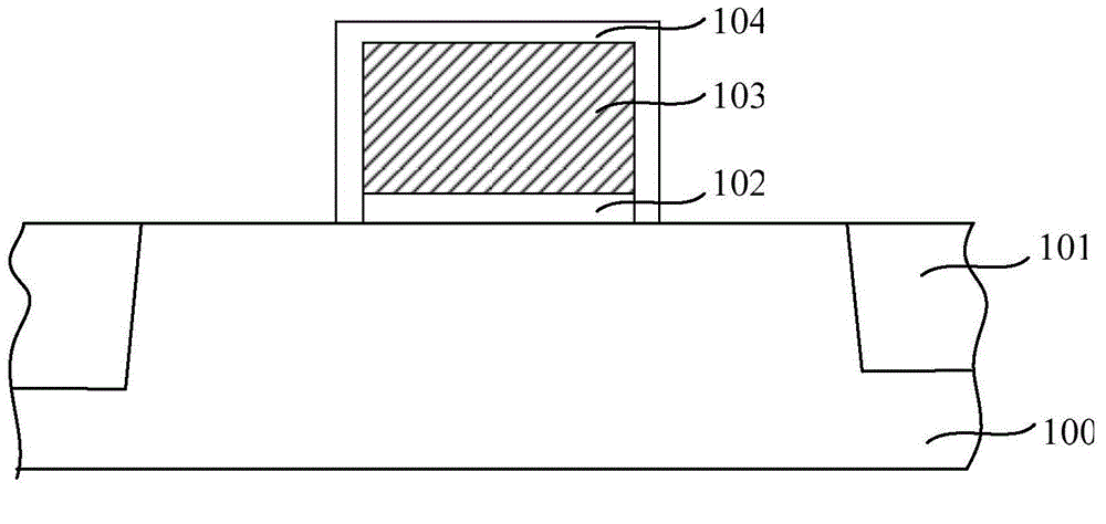
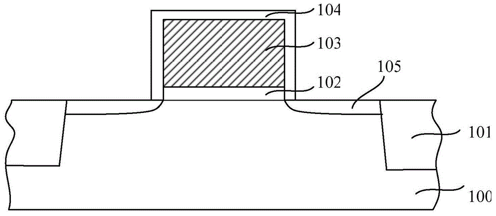
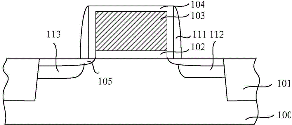
[0036] As mentioned in the background technology, the lightly doped region of the transistor formed in the prior art is difficult to meet the requirements of the process. The depth is still difficult to control.

[0037] Studies have found that in order to form a shallow doped region with a very shallow depth (15-30 angstroms), generally lower implantation energy (for example, less than 2Kev) is required, but ultra-low implantation energy (for example, less than 500ev) has a great impact on the implantation machine. The performance requirements of the MOS are improved, and the purchase of a new implantation machine will undoubtedly increase the production cost. In addition, depending on the type of implanted ions, the implantation depth is also difficult to control, especially in the production process of PMOS, by implanting boron ions to form ultra-shallow In the shallow doped region, because the mass of boron ions is relatively light and the particles are small, under the sa...


PUM


Abstract

The invention discloses a formation method of a semiconductor structure. The method comprises the steps of providing a semiconductor substrate which comprises a first region and a second region, forming a first gate structure on the semiconductor substrate in the first region, forming a second gate structure on the semiconductor substrate in the second region, forming a first photoresist layer covering the semiconductor substrate in the second region and the second gate structure, forming a second photoresist layer covering the semiconductor substrate in the first region and the first photoresist layer, performing shallow doping ion implantation on the semiconductor substrate on the two sides of the first gate structure in the first region by taking the second photoresist layer as a barrier layer, and forming a first shallow doping region in the semiconductor substrate on the two sides of the first gate structure. The method is suitable for forming a shallow doping region.

Description

technical field [0001] The invention relates to the field of semiconductor manufacturing, in particular to a method for forming a semiconductor structure. Background technique [0002] Metal-oxide-semiconductor (MOS) transistors are the most basic devices in semiconductor manufacturing. They are widely used in various integrated circuits. According to the main carrier and the type of doping during manufacturing, they are divided into NMOS and PMOS transistors. [0003] The prior art provides a method for manufacturing a MOS transistor. Please refer to Figure 1 to Figure 3 The schematic cross-sectional structure diagram of the formation process of the MOS transistor in the prior art is shown. [0004] Please refer to figure 1 , providing a semiconductor substrate 100, forming isolation structures 101 in the semiconductor substrate 100, the semiconductor substrate 100 between the isolation structures 101 is an active region, and forming a well region (not shown) in the act...

Claims


Application Information

Patent Timeline
Patent Type & Authority Applications(China)
IPC IPC(8): H01L21/266H01L29/78H01L21/8234
CPCH01L21/266H01L29/66477H01L29/78
Inventor 朱红波
Owner SEMICON MFG INT (SHANGHAI) CORP
Why Eureka
Try Eureka