Manufacturing method of power diode and power diode
A technology for power diodes and manufacturing methods, applied in semiconductor/solid-state device manufacturing, electrical components, circuits, etc., can solve problems such as reduction, Schottky diodes and PIN diodes cannot meet reverse blocking voltage and on-state voltage at the same time.
- Summary
- Abstract
- Description
- Claims
- Application Information
AI Technical Summary
Problems solved by technology
Method used
Image
Examples
Embodiment 1
[0036] This embodiment provides a method for manufacturing a power diode, including the following steps:
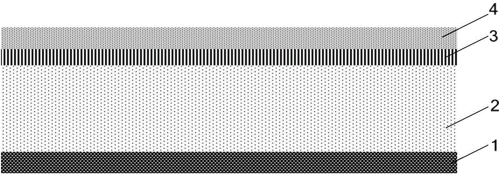
[0037] Step 1: As shown in FIG. 1(a), a semiconductor substrate 1 is provided, and an N-type epitaxial layer 2 is prepared on one side of the semiconductor substrate 1, and the other side of the semiconductor substrate 1 is used as a cathode of a power diode.
[0038] Step 2: As shown in FIG. 1(b), a silicon oxide layer 3 is prepared on the N-type epitaxial layer 2 by a thermal oxidation method.
[0039] Step 3: As shown in FIG. 1( c ), a polysilicon layer 4 is prepared on the silicon oxide layer 3 .
[0040] Step 4: As shown in Figure 1 (d), a photoresist mask is formed on the polysilicon layer 4, an etching window is formed at a preset position on the photoresist mask, and the silicon oxide layer 3 and the polysilicon are dry etched In layer 4, a trench is formed at a position corresponding to the etching window, so that the bottom of the trench is in contact with the ...
Embodiment 2
[0050]The present invention also provides a power diode manufactured according to the manufacturing method of Embodiment 1. The structure of the power diode is shown in FIG. 1(k). The structure of the power diode of this embodiment will be described in detail below.
[0051] In this embodiment, the first P-type ion implantation region 5 is formed in the N-type epitaxial layer 6 of the power diode corresponding to the position of the trench, and an N-type ion implantation region is formed in the first P-type ion implantation region 5 6 and the second P-type ion implantation region 7, and the N-type ion implantation region 5 is not in contact with the second P-type ion implantation region 7.
[0052] Further, the N-type ion implantation region 6 , the second P-type ion implantation region 7 , the first P-type ion implantation region 5 and the N-type epitaxial layer 6 form an NPN structure.
[0053] In this embodiment, a metal layer 9 is formed on the polysilicon layer 4 of the ...
PUM
 Abstract
Description
Claims
Application Information


