Packaging structure of MEMS (Micro Electro Mechanical Systems) chip integration

A packaging structure, ASIC chip technology, applied in the field of chip packaging, can solve the problems of large package size and signal input path product performance degradation, and achieve the effect of reducing size, reducing signal transmission path, and avoiding excessive substrate area

Inactive Publication Date: 2017-01-18
GOERTEK INC
View PDF6 Cites 5 Cited by
  • Summary
  • Abstract
  • Description
  • Claims
  • Application Information

AI Technical Summary

Problems solved by technology

[0006] In view of the above problems, the present invention provides a package structure for MEMS chip integration, to solve the problem that the package size of existing MEMS chip integration is too large, and the signal input path is too long to introduce parasitic effects, which leads to the degradation of product performance.

Method used


Image

  • Packaging structure of MEMS (Micro Electro Mechanical Systems) chip integration
  • Packaging structure of MEMS (Micro Electro Mechanical Systems) chip integration
  • Packaging structure of MEMS (Micro Electro Mechanical Systems) chip integration

Examples


Embodiment 1

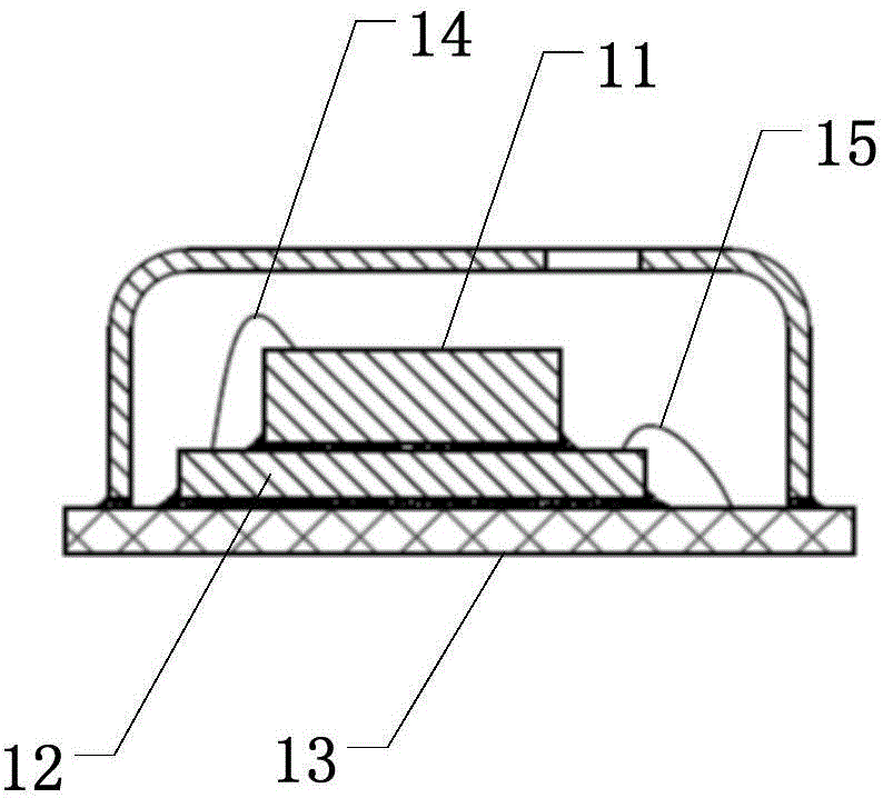
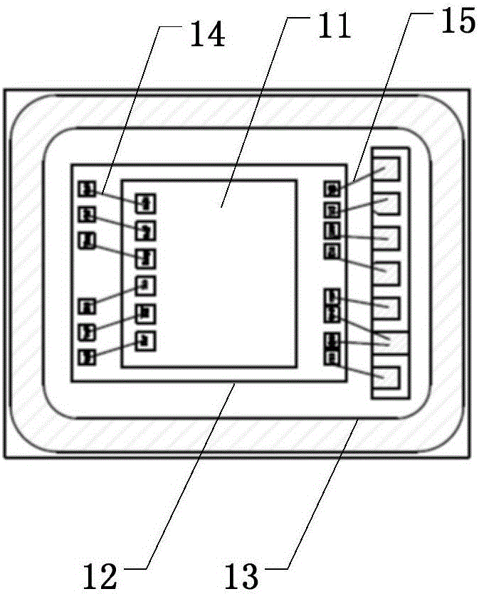
[0032] Embodiments of the present invention provide a MEMS chip integrated packaging structure, such as Figure 5 and Figure 6 As shown, the packaging structure includes: a substrate 33, a MEMS chip 31 and an ASIC chip 32, the MEMS chip 31 is arranged on the ASIC chip 32 in a stacked manner, the back of the ASIC chip 32 faces the substrate 33, and the back of the MEMS chip 31 faces The front side of the ASIC chip 32 .

[0033] The back side of the MEMS chip 31 and the front side of the ASIC chip 32 are mechanically connected by a patch adhesive layer. Both the front side of the MEMS chip 31 and the front side of the ASIC chip 32 have soldering pads 35, and the soldering pads 35 of the MEMS chip 31 and the soldering pads 35 of the ASIC chip 32 are A metal wire 34 is arranged between them to realize the electrical interconnection between the signal input of the ASIC chip 32 and the signal output of the MEMS chip 31, so that the signal of the MEMS chip 31 is output to the ASIC ...

Embodiment 2

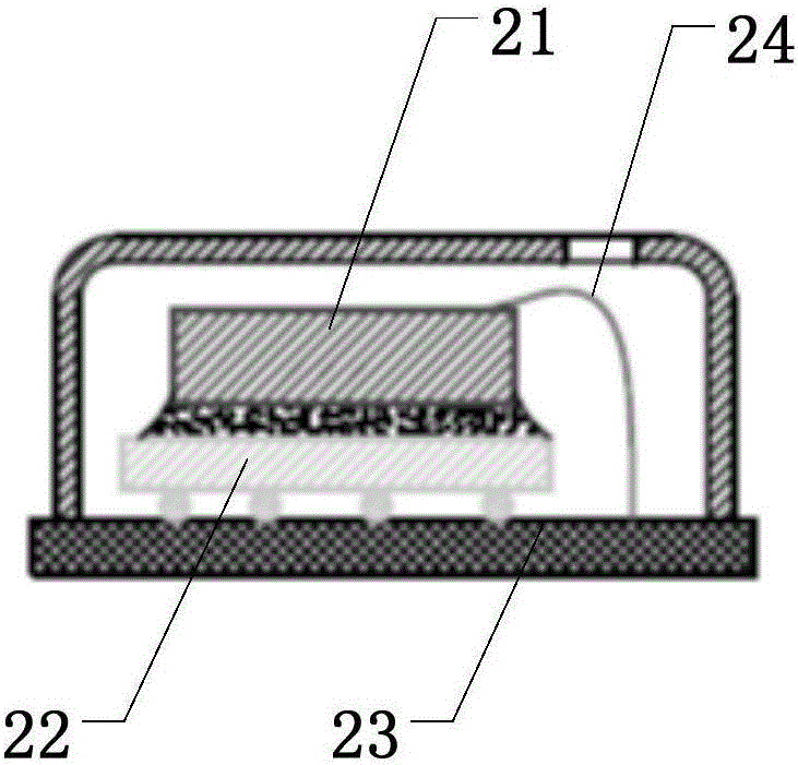
[0039] Such as Figure 7As shown, in the embodiment of the present invention, a number of TSVs 44 are formed on the MEMS chip 41, and the signal output on the front side of the MEMS chip 41 is guided to the back side through the TSVs 44; the back side of the MEMS chip 41 has a metal rewiring layer (not shown in the figure) and solder bumps 45 , the electrical interconnection between the MEMS chip 41 and the ASIC chip 42 is realized through the metal rewiring layer and the solder bumps 45 .

[0040] The packaging structure of the embodiment of the present invention further includes a plastic sealing layer 48, and the material of the plastic sealing layer 48 is a polymer or a film. The plastic encapsulation layer 48 covers the ASIC chip 42 and the MEMS chip 41 , fills the gap between the MEMS chip 41 and the ASIC chip 42 , and connects the ASIC chip 42 and the MEMS chip 41 together. During plastic sealing, care should be taken to protect the sensitive part of the chip from bein...


PUM


Abstract

The invention discloses a packaging structure of MEMS (Micro Electro Mechanical Systems) chip integration. On an ASIC (Application Specific Integrated Circuit) chip, a silicon through hole is manufactured to lead signal output on the front side of the ASIC chip to the back surface of the ASIC chip, and the electrical interconnection of the ASIC chip and a base plate is realized through a metal re-wiring layer and solder bumps on the back surface. According to the way, a signal transmission path is reduced, meanwhile, a phenomenon that a lead bonding connection way requires an overlarge base plate area is avoided, and the size of the packaging structure is reduced. The front side of the MEMS chip and the front side of the ASIC chip are electrically connected directly through a metal lead to guarantee the minimum path of signal transmission and avoid introducing stray capacitance. Or a silicon through hole technology is used for leading the signal output on the front side of the MEMS chip to the back surface of the MEMS chip, then the electric interconnection of the MEMS chip and the ASIC chip is realized through the metal re-wiring layer and the solder bumps, furthermore, the signal transmission path is reduced, and the connection way of lead bonding is completely avoided so as to further reduce the size of the packaging structure of the chip.

Description

technical field [0001] The invention relates to the technical field of chip packaging, in particular to a packaging structure for MEMS chip integration. Background technique [0002] Micro Electro Mechanical Systems (MEMS) refers to micro electromechanical systems that integrate micro sensors, actuators, signal processors, control circuits, interface circuits, communications and power supplies. To realize specific functions of the MEMS chip, an application specific integrated circuit (Application Specific Integrated Circuits, ASIC) chip is needed, and the ASIC chip processes the collected signals output by the MEMS. In MEMS packaging in the prior art, a single MEMS chip and ASIC chip are usually packaged based on a substrate to achieve corresponding functions, such as capacitive pressure sensors, capacitive temperature sensors, capacitive humidity sensors, MEMS microphones, and the like. [0003] Generally speaking, in order to obtain a larger capacitance output signal, red...

Claims


Application Information

Patent Timeline
Patent Type & Authority Applications(China)
IPC IPC(8): B81B7/00
CPCB81B7/0006
Inventor 张俊德
Owner GOERTEK INC
Why Eureka
Try Eureka