Formation method of semiconductor structure

A semiconductor and gas technology, which is applied in the manufacture of semiconductor/solid-state devices, electrical components, circuits, etc., can solve the problems of semiconductor structure electrical properties that need to be improved, and achieve the effects of increasing the forming process window, close contact, and reducing resistivity

Active Publication Date: 2017-02-15
SEMICON MFG INT (SHANGHAI) CORP +1
View PDF6 Cites 6 Cited by
  • Summary
  • Abstract
  • Description
  • Claims
  • Application Information

AI Technical Summary

Problems solved by technology

[0004] However, the electrical properties of semiconductor stru

Method used


Image

  • Formation method of semiconductor structure
  • Formation method of semiconductor structure
  • Formation method of semiconductor structure

Examples


Embodiment Construction

[0034] It can be seen from the background art that the electrical performance of the semiconductor structure formed in the prior art needs to be improved.

[0035] In one embodiment, the forming process of the semiconductor structure includes the following steps:,

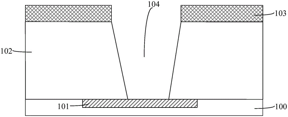
[0036] refer to figure 1 , providing a substrate 100, wherein an underlying metal layer 101 is formed in the substrate 100; a dielectric layer 102 is formed on the surface of the underlying metal layer 101 and the surface of the substrate 100; a patterned mask layer 103 is formed on the surface of the dielectric layer 102; The dielectric layer 102 is etched using the patterned mask layer 103 as a mask to form an opening 104 penetrating through the dielectric layer 102 , and the opening 104 exposes the top surface of the underlying metal layer 101 .

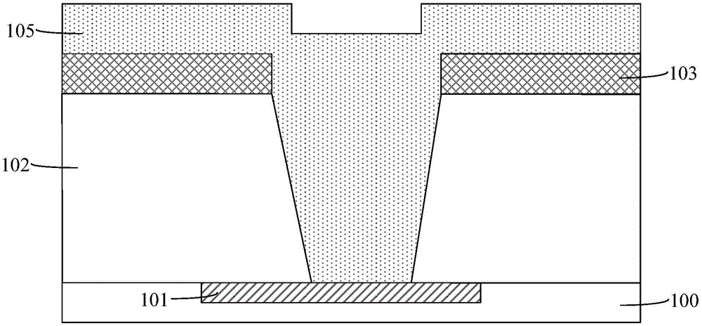
[0037] refer to figure 2 , forming to fill the opening 104 (refer to figure 1 ), and the conductive film 105 is also located on the surface of the patterned mask l...


PUM


Abstract

A formation method of a semiconductor structure comprises the steps of providing a substrate in which a bottom-layer metal layer is formed; forming a dielectric layer covering the surfaces of the substrate and the bottom-layer metal layer, wherein the material of the dielectric layer has a porous structure; forming a patterned mask layer on the surface of the dielectric layer; taking the patterned mask layer as a mask to etch the dielectric layer, forming an opening penetrating the dielectric layer, and exposing the top surface of the bottom-layer metal layer out of the bottom of the opening; adopting a carbon-containing gas to carry out the first etching postprocessing on the opening, and forming a sealing layer on the surface of the side wall of the opening; after the sealing layer is formed, adopting a wet etching process to etch and remove the patterned mask layer; forming a conductive layer filling the opening, wherein the top of the conductive layer is parallel and level with the top of the dielectric layer. According to the present invention, a technical window for forming the conductive layer is added, and the electrical property of the semiconductor structure is improved.

Description

technical field [0001] The invention relates to the technical field of semiconductor manufacturing, in particular to a method for forming a semiconductor structure. Background technique [0002] With the continuous advancement of VLSI process technology, the feature size of semiconductor devices has been continuously reduced, and the chip area has continued to increase. The delay time of the interconnect structure can be compared with the device gate delay time. People are faced with the problem of how to overcome the significant increase in RC (R refers to resistance, C refers to capacitance) delay due to the rapid increase in connection length. In particular, due to the increasing influence of the capacitance between metal wirings, the performance of the device is greatly reduced, which has become a key restrictive factor for the further development of the semiconductor industry. In order to reduce the RC delay caused by interconnection, various measures have been adopted...

Claims


Application Information

Patent Timeline
IPC IPC(8): H01L21/768
CPCH01L21/76802H01L21/76807H01L21/76814H01L21/76877
Inventor 张海洋周俊卿袁光杰
Owner SEMICON MFG INT (SHANGHAI) CORP
Why Eureka
Try Eureka