Grain-oriented electrical steel sheet and manufacturing method thereof
An electromagnetic steel plate and manufacturing method technology, applied in the direction of manufacturing tools, inorganic material magnetism, electron beam welding equipment, etc., can solve problems such as deterioration of iron loss characteristics, bending of steel plates, discontinuous beam irradiation area, etc., and achieve iron loss Excellent properties and the effect of suppressing the increase of iron loss
- Summary
- Abstract
- Description
- Claims
- Application Information
AI Technical Summary
Problems solved by technology
Method used
Image
Examples
Embodiment 1
[0113] A cold-rolled steel sheet containing Si: 3% by mass, with a final thickness of 0.23 mm and a width of 1250 mm, was subjected to primary recrystallization annealing that doubles as decarburization annealing, and then an annealing separator mainly composed of MgO was applied to the surface of the steel sheet. , implement final annealing including secondary recrystallization annealing and purification annealing, make grain-oriented electrical steel sheet with forsterite film, and then coat 60% by mass of insulating coating formed by colloidal silica and aluminum phosphate, implement Sintering was performed by planarizing annealing at a temperature of 800°C.
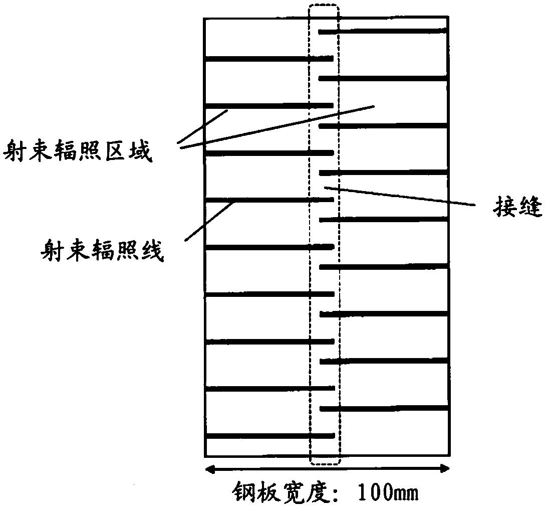
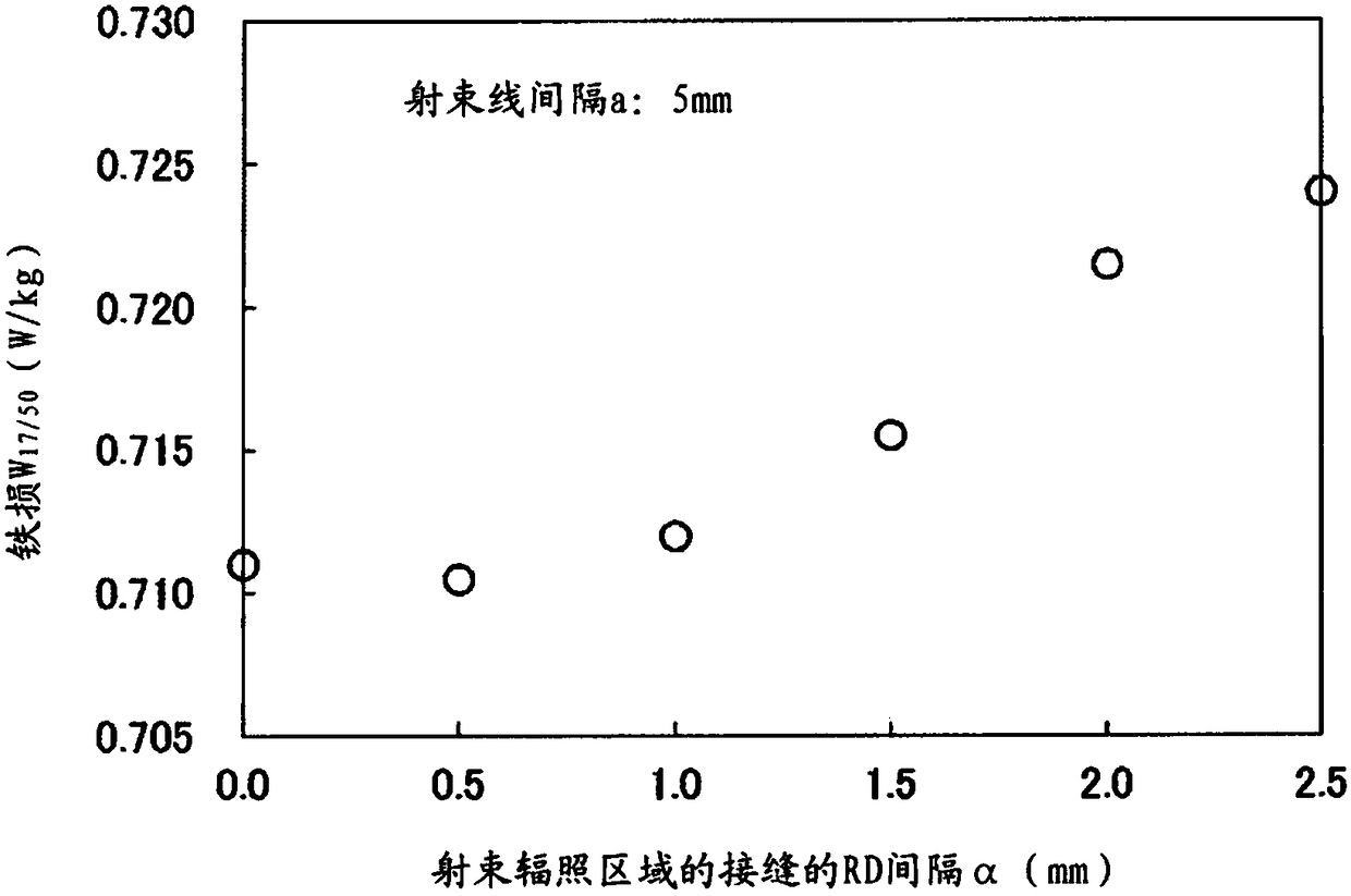
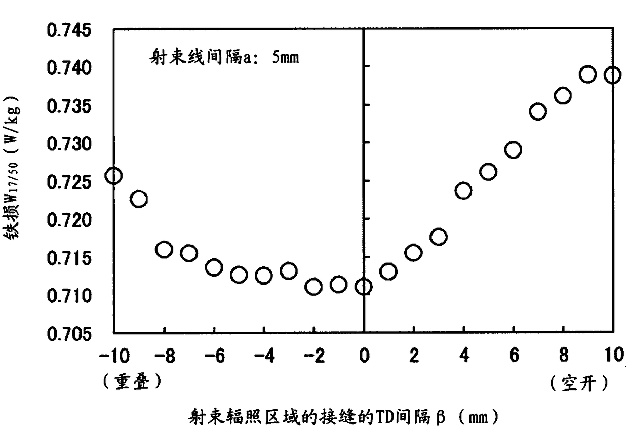
[0114] Next, the above-mentioned steel plate is irradiated continuously in a line with laser light in a direction at right angles to the rolling direction by using 4 fiber lasers installed in the width direction of the steel plate, or irradiated by 8 electron beams installed in the width direction of the steel plate T...
Embodiment 2
[0123] Using 6 electron beam irradiation devices installed in the width direction of the steel sheet, electron beams were irradiated to the grain-oriented electrical steel sheet with a final sheet thickness of 0.23 mm x a sheet width of 1250 mm and a coil length of 5000 m after forming an insulating film to perform magnetic domain refinement. treatment. At this time, the target β value was changed so that the TD interval β of the seam of the beam irradiation region was -5 mm, -3 mm, 0 mm, and 3 mm, and the electron beam was irradiated in such a manner.
[0124] Then, a total of 51 test pieces were collected from the product coil every 100m, and the TD interval β of the seam in the beam irradiation area was measured, and the maximum and minimum values of the TD interval β of the 51 samples measured were shown in Table 2. From the results, it can be seen that by setting the target value of the TD interval β at -3 to 0 mm and performing beam irradiation, the range of the TD in...
PUM
| Property | Measurement | Unit |
|---|---|---|
| thickness | aaaaa | aaaaa |
Abstract
Description
Claims
Application Information


