

Flip chip interconnection process method for high frequency chip waveguide package
A process method and chip technology, applied in the direction of semiconductor devices, semiconductor/solid-state device manufacturing, electrical components, etc., to achieve the effect of reducing package size, small bonding size, and good controllability of coherent parameters
- Summary
- Abstract
- Description
- Claims
- Application Information
AI Technical Summary
Problems solved by technology
Method used
Image

Examples
Embodiment 1
[0051] Such as Figure 1-7 As shown, when a special-shaped microstrip line substrate is used, the specific package flip-chip interconnection process steps are as follows:
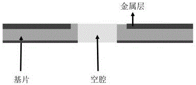
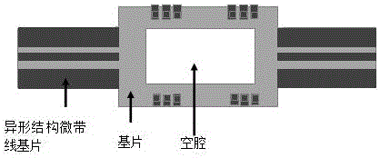
[0052] First, according to the size of the chip and its pad, and the performance design parameters of the corresponding functional modules, the size, cavity and irregular boundary structure of the special-shaped microstrip line substrate are designed and manufactured;
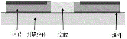
[0053] Then, use solder to flatly mount the microstrip line substrate on the surface of the package cavity;
[0054] Then according to the size of the chip pad, make flip-chip solder bumps on the chip pad;
[0055] Finally, flip-chip bonding technology is used to realize the interconnection between the chip and the microstrip line substrate.
[0056] In the steps of this interconnection process, based on the structural design of the special-shaped microstrip line substrate, the microstrip line structure is fabricated on the quartz substrat...
Embodiment 2
[0064] Such as Figure 8-14 As shown, when flip-chip interconnection is used, the specific package flip-chip interconnection process steps are as follows:
[0065] 1. According to the packaging design requirements, select the appropriate material to make the supporting substrate of the chip and the microstrip line substrate;
[0066] 2. According to the size of the chip and the microstrip line substrate, make a groove on the substrate for placing the chip and the microstrip line substrate, the purpose is to fix the position of the chip and the microstrip line substrate during flip-chip welding, and at the same time Ensure the flatness of the patch;
[0067] 3. Mount the chips and microstrip line substrates flatly in the substrate grooves to ensure the high flatness requirements of the flip-chip welding technology for the samples;
[0068] 4. According to the size and spacing of chip pads, the size and spacing of microstrip line substrate pads, and the corresponding functiona...
PUM
 Abstract
Description
Claims
Application Information