Mounting structure and method for producing mounting structure

A structure and assembly surface technology, which is applied in semiconductor/solid-state device manufacturing, printed circuit manufacturing, printed circuit assembly of electrical components, etc., can solve problems such as unclear connection reliability of solder joints

Active Publication Date: 2017-02-22
PANASONIC INTELLECTUAL PROPERTY MANAGEMENT CO LTD
View PDF6 Cites 3 Cited by
  • Summary
  • Abstract
  • Description
  • Claims
  • Application Information

AI Technical Summary

Problems solved by technology

However, for BGA connections using Sn-Zn-based, Sn-Ag-In-based, and Sn-Bi-based solders, the connection reliability of the solder connection is still unclear.

Method used


Image

  • Mounting structure and method for producing mounting structure
  • Mounting structure and method for producing mounting structure
  • Mounting structure and method for producing mounting structure

Examples


Embodiment approach 1

[0037] The assembled structure of Embodiment 1 is as image 3 shown.

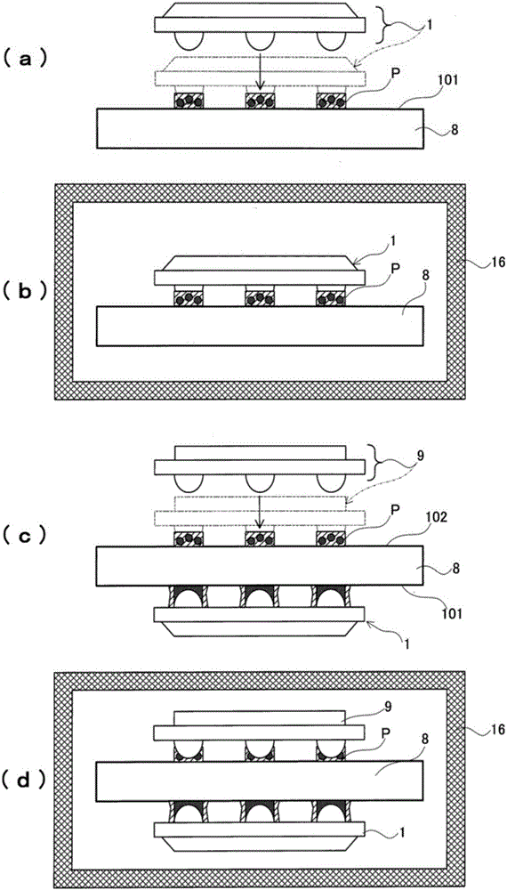
[0038] In this assembled structure, the components and the like of the solder paste used are selected. Thus only by implementing figure 1 (a)~ figure 1The same process described in (d) can produce a good assembled structure.

[0039] To explain, to express the existing example figure 1 (a)~ figure 1 (d), figure 2 (a), figure 2 (b) The same parts are described with the same symbols.

[0040] In this assembly structure, the semiconductor element 1 as the first assembly component is solder-assembled on the primary assembly surface 101 of the circuit board 8 as the component to be assembled, and the semiconductor element 1 as the second assembly component is solder-assembled on the secondary assembly surface 102 of the circuit substrate 8. The semiconductor element 9 is formed.

[0041] Hemispherical bumps 4 are formed on the electrodes 3 formed on the substrate 2 of the semiconductor element 1 . Th...

Embodiment approach 2

[0052] Figure 4 The assembly structure of Embodiment 2 is shown.

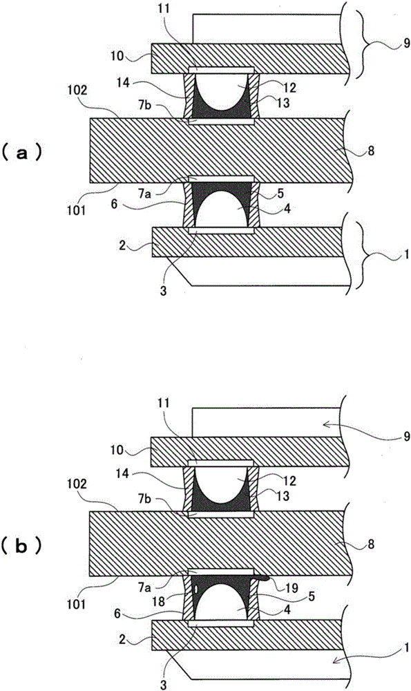
[0053] exist image 3 In the illustrated first embodiment, the vertices of the bumps 4 of the semiconductor element 1 do not directly contact the electrodes 7 a of the primary mounting surface 101 of the circuit board 8 . In addition, cured solder 5 is interposed between the apex of the bump 4 and the electrode 7 a. On the other hand, in the second embodiment, the apexes of the bumps 4 of the semiconductor element 1 are directly in contact with the electrodes 7 a of the primary mounting surface 101 of the circuit board 8 . Other than that, it is the same as Embodiment 1.

[0054] ie, with image 3 In the same way as in the case of , the solder 5 and half of the entire surface of the bump 4 are not covered with the reinforcing resin 6 . An exposed portion Oa exposing a part of the solder 5 is formed. with Embodiment 1 image 3 The difference is that the apex of the bump 4 is in contact with the electrode...

Embodiment approach 3

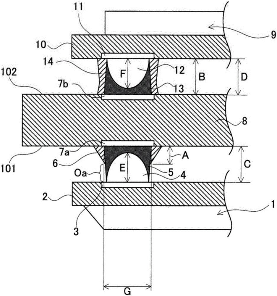
[0058] Figure 5 The assembly structure of Embodiment 3 is shown.

[0059] exist image 3 In the assembly structure according to Embodiment 1 shown, the semispherical bump 4 is formed on the electrode 3 of the semiconductor element 1 . But when Figure 5 In the assembled structure of the semiconductor device 1, spherical bumps 41 are used on the electrodes 3 of the semiconductor element 1. Only this point is different from image 3 different. Other than that, it is the same as Embodiment 1. That is, the apex of the reinforcing resin 6 does not come into contact with the bump 41, and the exposed portion Oa where a part of the solder 5 is exposed is not in contact with the bump 41. image 3 The situation is similarly formed. The composition of the bump 41 is the same as that of the bump 4 .

[0060] Therefore, the ratio of the gap width C between the circuit substrate 8 and the substrate 2 image 3 The gap in the situation is much larger. Therefore, the strength is weak...


PUM


Abstract

The invention provides a mounting structure capable of preventing flashing of a solder during two-surface mounting, and a method for producing the mounting structure. The mounting structure is characterized in that a mounting part (1) is mounted on a mounting surface (101) of a member to be mounted (8), and a mounting part (9) is mounted on a mounting surface (102) of the member to be mounted (8). The mounting structure includes: reinforcing resin, wherein a base end of the reinforcing resin is connected to the mounting surface (101) of the member to be mounted (8) so as to cover a part of a solder (5), and a front end of the reinforcing resin does not contact a bump (4); a part of the solder (5) forms an exposed portion (Oa) between the front end of the reinforcing resin (6) and a substrate (2) of the mounting part (1), and the exposed portion is exposed, accordingly, the re-molten solder (5) expands outward from the exposed portion (Oa) through secondary backflow when the mounting part (9) is mounted on the mounting surface (102) of the member to be mounted (8), and the solder (5) returns to an original position through cooling.

Description

technical field [0001] The present invention relates to an assembly structure in which assembly components such as a semiconductor chip with solder bumps, a semiconductor package, and an electronic component with solder bumps are mounted on both surfaces of assembly components such as a circuit board. Background technique [0002] In recent years, portable devices such as mobile phones and PDAs (Personal Digital Assistants) have been miniaturized and highly functional. As a package technology that can cope with this, many package structures such as BGA (Ball Grid Array) and CSP (Chip Scale Package) are used. Portable devices are susceptible to mechanical loads such as drop shocks. QFP (Quad FlatPackage) absorbs shock with its wire part. However, in BGAs, CSPs, and the like that do not have lead wires for cushioning shocks, it is important to ensure reliability against shocks. [0003] The melting point of Pb eutectic solder, which is a typical conventional solder, is 183°...

Claims


Application Information

Patent Timeline
Patent Type & Authority Applications(China)
IPC IPC(8): H01L21/60H01L21/56H01L23/31H05K3/34
CPCH01L21/56H01L23/31H01L24/14H01L24/81H05K3/34H05K3/3457H01L2224/1405H01L2224/141H01L2224/818H01L2224/81815H01L24/16H01L25/105H01L25/50H01L2225/1023H01L2225/1058H01L2225/107H01L2924/15311H01L24/13H01L2224/10156H01L2224/13111H01L2224/133H01L2224/1601H01L2224/16058H01L2224/81191H01L2224/81193H01L2224/8121H01L2924/3841H01L2224/8159H01L2224/816H01L2224/1329H01L2224/16505H01L25/0657H01L2225/06517H01L2225/06572H01L2924/014H01L2924/00012H01L2924/01047H01L2924/01029H01L21/4853H01L23/49816H01L2021/60007
Inventor 日野裕久铃木康宽森将人大桥直伦
Owner PANASONIC INTELLECTUAL PROPERTY MANAGEMENT CO LTD
Why Eureka
Try Eureka