Supercharge Your Innovation With Domain-Expert AI Agents!

GaN-based hybrid PIN Schottky diode and production method thereof

A Schottky diode and electrode technology, which is applied in semiconductor/solid-state device manufacturing, electrical components, circuits, etc., can solve the problems that the effect cannot meet the requirements, and achieve the effect of reducing the peak electric field intensity and increasing the breakdown voltage

Inactive Publication Date: 2017-02-22
FUDAN UNIV
View PDF5 Cites 6 Cited by
  • Summary
  • Abstract
  • Description
  • Claims
  • Application Information

AI Technical Summary

Problems solved by technology

However, GaN-based MPS devices with traditional structures cannot fully utilize the advantages of GaN materials, and their breakdown field strength is often only half of the critical breakdown field strength.
The breakdown voltage of the device can be improved by using termination techniques such as field plates and field limiting rings, but the effect cannot meet the requirements in some cases

Method used


Image

  • GaN-based hybrid PIN Schottky diode and production method thereof
  • GaN-based hybrid PIN Schottky diode and production method thereof
  • GaN-based hybrid PIN Schottky diode and production method thereof

Examples


Embodiment Construction

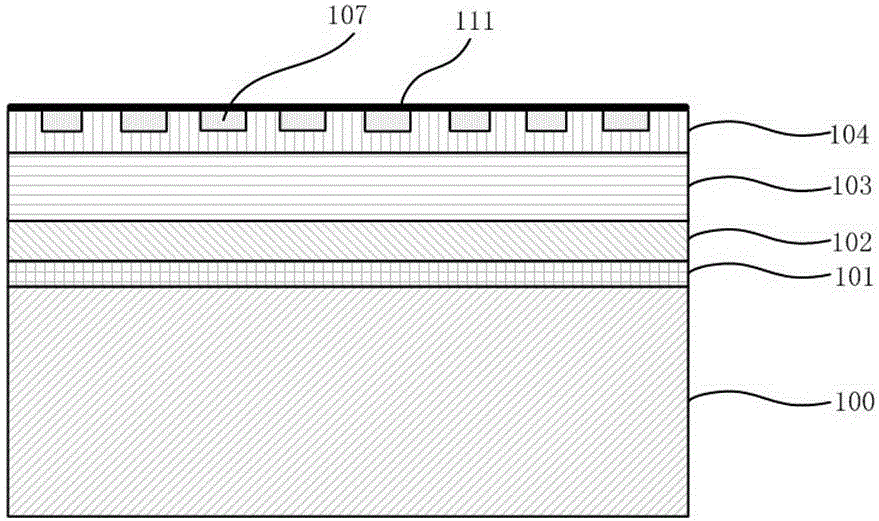
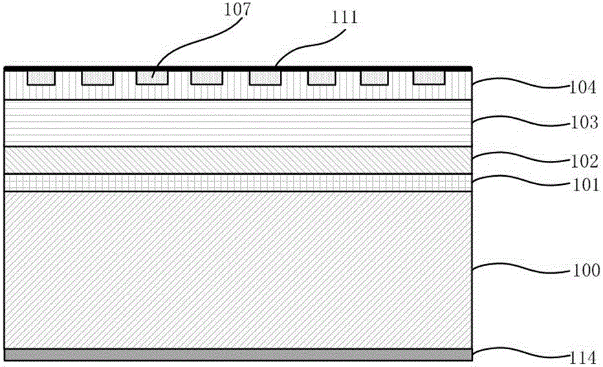
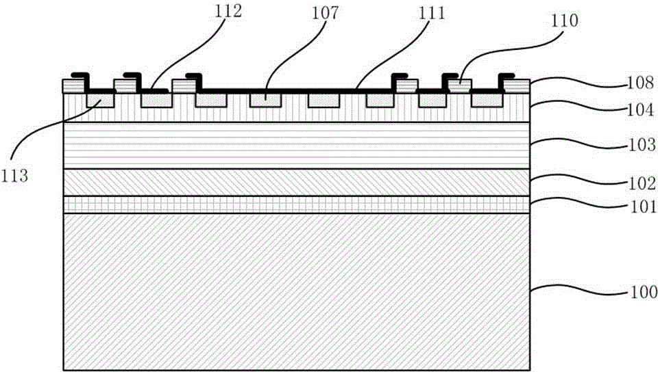
[0035] Embodiments of the present invention will be described in detail below with reference to the accompanying drawings, in which like elements are denoted by like reference numerals. The embodiments described below are exemplary, and in order to simplify the disclosure of the present invention, components and arrangements of specific examples are described below. Of course, these are only examples for the purpose of explaining the present invention and should not be construed as limiting the present invention. In addition, the present invention provides various specific examples of processes and materials, but the invention may be practiced without these specific details, as will be understood by those skilled in the art. Unless otherwise specified below, each part of the device can be implemented using processes and materials known in the art. Additionally, configurations described below in which a first feature is "on" a second feature may include embodiments where the f...


PUM


Abstract

The invention belongs to the technical field of semiconductors and particularly relates to a GaN-based hybrid PIN Schottky diode and a production method thereof. The GaN-based hybrid PIN Schottky diode comprises an n-type GaN substrate, an n-type GaN drift layer positioned on the GaN substrate and having multilayer structure with layers decreasing gradually in doping concentration from bottom top, a plurality of p-type GaN structural layers distributed in the top layer of the multilayer-structure n-type GaN drift layer in certain intervals, and a main junction electrode formed on the n-type GaN drift layer between the multiple p-type GaN structural layers and the p-type GaN structural layers and in Schottky contact with the n-type GaN drift layer. By introducing multilayer drift region technology, it is possible to effectively reduce peak electric field intensity of p-n junction interfacial attachments, and breakdown voltage of a device can be increased at the premise of acquiring reasonable forward current.

Description

technical field [0001] The invention belongs to the technical field of semiconductors, and in particular relates to a GaN-based mixed PIN Schottky diode and a preparation method thereof. Background technique [0002] As the most widely used third-generation semiconductor material, GaN has a larger band gap, higher critical breakdown field strength and saturated electron velocity, better thermal and chemical stability, and better thermal conductivity. sex. These properties make GaN have broad application prospects in the fields of high temperature, high frequency and high power devices. The quality factor of GaN-based power devices can even be an order of magnitude higher than that of Si-based devices. GaN devices currently mainly include metal-oxide-semiconductor field-effect transistors (MOSFETs), metal-semiconductor field-effect transistors (MESFETs), and high electron mobility transistors (HEMTs), among which HEMTs are the most widely used, and hybrid PIN Schottky (MPS ...

Claims


Application Information

Patent Timeline
Patent Type & Authority Applications(China)
IPC IPC(8): H01L29/872H01L21/329
CPCH01L29/872H01L29/66143
Inventor 陈琳郑亮戴亚伟孙清清张卫
Owner FUDAN UNIV
Features
  • R&D
  • Intellectual Property
  • Life Sciences
  • Materials
  • Tech Scout
  • Unparalleled Data Quality
  • Higher Quality Content
  • 60% Fewer Hallucinations
Learn More