Field effect transistor device

A technology of field effect transistors and devices, applied in the field of microelectronics, to achieve the effects of reducing leakage current, reducing peak electric field intensity, and reducing peak electric field

Active Publication Date: 2020-06-26
INST OF SEMICONDUCTORS - CHINESE ACAD OF SCI
View PDF6 Cites 0 Cited by
  • Summary
  • Abstract
  • Description
  • Claims
  • Application Information

AI Technical Summary

Problems solved by technology

The defect of the existing field plate structure is that the breakdown of the insulating medium (that is, the field plate passivation layer) becomes a new limitation for the improvement of the breakdown voltage of the device

Method used


Image

  • Field effect transistor device
  • Field effect transistor device

Examples


specific Embodiment approach

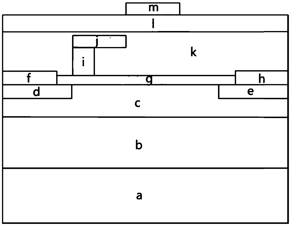
[0062] Specific implementation methods include:

[0063] A method for manufacturing a high-voltage-resistant field-effect transistor provided in this embodiment, the specific process is as follows:

[0064] (1) Clean the substrate: Ga 2 o 3 The semi-insulating substrate material was boiled with acetone and ethanol for 10 minutes, then washed with deionized water for 30 times, and finally dried with high-purity nitrogen;

[0065] (2) Epitaxial growth: put the cleaned substrate into MOCVD equipment, and grow Si-doped Ga of 100nm-300nm by controlling the process parameters. 2 o 3 channel layer;

[0066] (3) Ion implantation and annealing treatment: Firstly, photolithography is performed on the sample to form a pattern window of the source and drain regions, then ion implantation is performed on the source and drain ohmic contact regions, and then annealing treatment is performed at 950°C for 30 minutes in a nitrogen atmosphere. Then the sample is cleaned according to the met...


PUM

PropertyMeasurementUnit
thicknessaaaaaaaaaa
thicknessaaaaaaaaaa
lengthaaaaaaaaaa

Abstract

The invention discloses a field effect transistor device, and the device comprises a composite passivation layer which comprises a first passivation layer which is disposed on a gate dielectric layerof a field effect transistor, and covers a source electrode, a drain electrode and a gate electrode of the field effect transistor; a second passivation layer arranged on the first passivation layer;a transverse field plate arranged to be in contact with the gate electrode and arranged in the first passivation layer; and a floating field plate arranged on the second passivation layer. According to the field effect transistor device provided by the invention, the composite passivation layer with a two-layer structure is designed, the structure of the composite passivation layer is the first passivation layer/ the second passivation layer, the first passivation layer is used as a transverse field plate passivation layer, and the second passivation layer is used as a passivation layer of thefloating field plate. By designing the parameters of the transverse field plate, the floating field plate and the composite passivation layer, the peak electric fields of the gate dielectric layer and the field plate passivation layer are effectively reduced, and the breakdown voltage of a gallium oxide monopole device is improved.

Description

technical field [0001] The invention relates to the technical field of microelectronics, in particular to a field effect transistor device with high voltage resistance. Background technique [0002] Gallium oxide (Ga 2 o 3 ) has a bandgap of 4.2-4.9eV, and is a direct bandgap III-V group ultra-wide bandgap semiconductor material with excellent chemical and thermal stability. Due to its excellent physical properties and chemical stability, it has great potential in the application of optoelectronic devices such as high voltage resistance, low loss, high power, high temperature resistance and solar blindness, such as high-power field effect transistors and semiconductor photodetectors, etc. And it can play an important role in harsh environments such as aviation and aerospace. Ga 2 o 3 As a fourth-generation semiconductor material, it has the characteristics of large band gap, high breakdown field strength, and low conduction power consumption, and is especially suitable ...

Claims


Application Information

Patent Timeline
Patent Type & Authority Applications(China)
IPC IPC(8): H01L29/40H01L29/786H01L21/34
CPCH01L29/404H01L29/405H01L29/66969H01L29/78606H01L29/7869
Inventor 马培培郑军成步文
Owner INST OF SEMICONDUCTORS - CHINESE ACAD OF SCI
Why Eureka
Try Eureka