DMOS transistor containing field plate and manufacturing method thereof

A transistor and field plate technology, applied in the field of DMOS devices and their fabrication, can solve problems such as reducing device performance, and achieve the effects of increasing electric field distribution length, improving performance, and reducing possibility

Active Publication Date: 2022-06-24
江苏游隼微电子有限公司
View PDF3 Cites 0 Cited by
  • Summary
  • Abstract
  • Description
  • Claims
  • Application Information

AI Technical Summary

Problems solved by technology

[0003] In the DMOS device design process, the breakdown voltage and on-resistance of the device are very important parameters. During the conduction process of the prior art device, when the carriers flow from the metallized source to the metallized drain, when the When the gate electrode voltage continues to increase to a certain value, the carriers will tunnel into the gate through the quality defects of the oxide layer, resulting in gate-source conduction and reducing the performance of the device.

Method used


Image

  • DMOS transistor containing field plate and manufacturing method thereof
  • DMOS transistor containing field plate and manufacturing method thereof
  • DMOS transistor containing field plate and manufacturing method thereof

Examples


Embodiment Construction

[0026] The present invention will be further explained below in conjunction with the accompanying drawings.

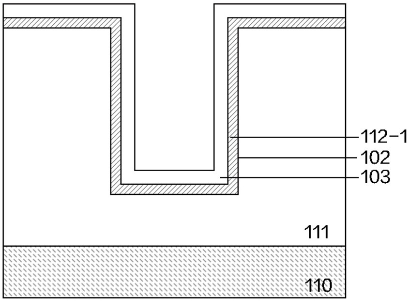
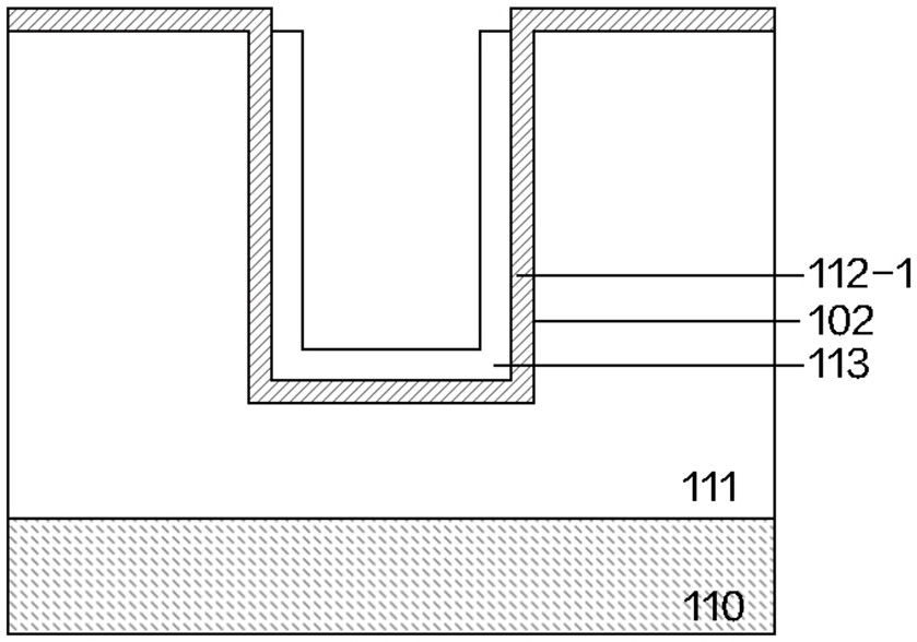
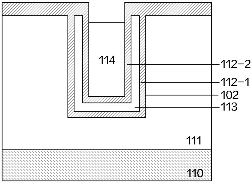
[0027] like figure 1 As shown, a DMOS transistor with a field plate includes a metallized drain 100 , an N-type heavily doped substrate 110 , and an N-type drift region 111 , which are sequentially stacked from bottom to top.

[0028] A deep trench structure 102 is provided in the N-type drift region 111, and the deep trench structure 102 includes a first oxide layer 112-1, a second oxide layer 112-2, a third oxide layer 112-3, and a fourth oxide layer 112-4. The first oxide layer 112 - 1 is a U-shaped structure embedded in the N-type drift region 111 , and the upper surface of the first oxide layer 112 - 1 is flush with the upper surface of the N-type drift region 111 . The second oxide layer 112-2 has a U-shaped structure inside the first oxide layer 112-1, and the first oxide layer 112-1 and the second oxide layer 112-2 are isolated by a U-shaped field plate 113. ...


PUM


Abstract

According to the DMOS transistor containing the field plate and the manufacturing method of the DMOS transistor containing the field plate, a U-shaped field plate is additionally arranged between a gate electrode and a source region, a field plate electrode is formed by depositing metal, the potential of the field plate electrode is adjusted, and it is avoided that under large voltage, carriers enter the gate electrode in a tunneling mode through oxide layer quality defects, and consequently gate source conduction is caused. And meanwhile, the U-shaped field plate structure can also increase the electric field distribution length, so that the effects of reducing the peak electric field intensity and dispersing the peak electric field of the device are achieved, the breakdown voltage of the DMOS device is further improved, and the on-resistance is further reduced.

Description

technical field [0001] The invention relates to a semiconductor device and a manufacturing method, in particular to a DMOS device and a manufacturing method thereof. Background technique [0002] With the continuous development of the semiconductor industry, high performance and miniaturization have become the development trend of electronic systems. Among them, the two key parameters of power MOSFET (Metal Oxide Semiconductor Field-Effect Transistor) are breakdown voltage and on-resistance. Since the MOSFET device is a single-stage device, its breakdown voltage is related to the thickness of the drift region and the doping concentration of the drift region. A high breakdown voltage requires a thick drift region and a low doping concentration of the drift region, which will make it turn on resistance increases. Therefore, as the withstand voltage of the device increases, the on-resistance increases exponentially, and the power consumption increases greatly. In particular,...

Claims


Application Information

Patent Timeline
Patent Type & Authority Applications(China)
IPC IPC(8): H01L29/40H01L29/78H01L21/336
CPCH01L29/7813H01L29/66734H01L29/407
Inventor 吴李瑞王彬徐凯程晨张永生
Owner 江苏游隼微电子有限公司
Why Eureka
Try Eureka