OLED (organic light emitting diode) displaying device and manufacturing method thereof

A technology for a display device and a manufacturing method, which is applied in the manufacturing of semiconductor/solid-state devices, organic semiconductor devices, electrical components, etc., can solve the problems of reducing the service life of OLED display devices, accelerating the deterioration rate of materials, and unfavorable heat, and avoiding OLED materials. The effect of accelerating deterioration rate, avoiding accelerated deterioration rate, and increasing heat transfer rate

Inactive Publication Date: 2017-02-22
WUHAN CHINA STAR OPTOELECTRONICS TECH CO LTD
View PDF7 Cites 16 Cited by
  • Summary
  • Abstract
  • Description
  • Claims
  • Application Information

AI Technical Summary

Problems solved by technology

Because the luminous efficiency of the OLED device 20 often cannot reach 100% when it is working, a large part of the electric energy will be converted into heat energy, but the thermal conductivity of the buffer layer 32 made of organic materials in the thin film encapsulation layer 30 is low, which is not conducive to heat dissipation. The transfer of heat will cause the temperature of the OLED device 20 to rise continuously due to the accumulation of heat during operation, resulting in accelerated deterioration of the materials of the OLED device 20 and reducing the service life of the OLED display device.

Method used


Image

  • OLED (organic light emitting diode) displaying device and manufacturing method thereof
  • OLED (organic light emitting diode) displaying device and manufacturing method thereof
  • OLED (organic light emitting diode) displaying device and manufacturing method thereof

Examples


Embodiment Construction

[0028] In order to further illustrate the technical means adopted by the present invention and its effects, the following describes in detail in conjunction with preferred embodiments of the present invention and accompanying drawings.

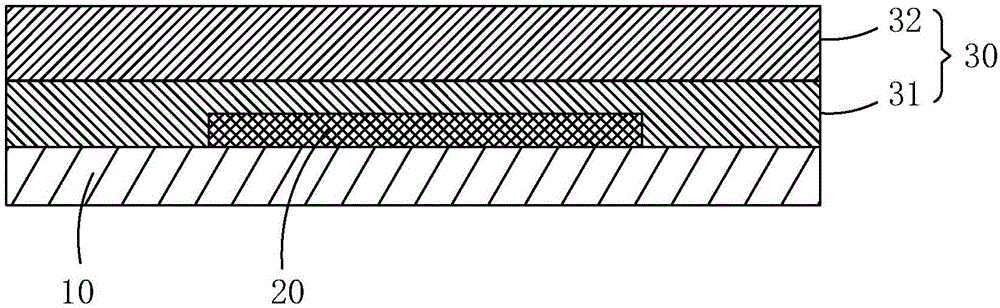
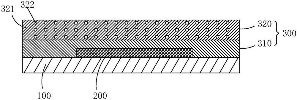
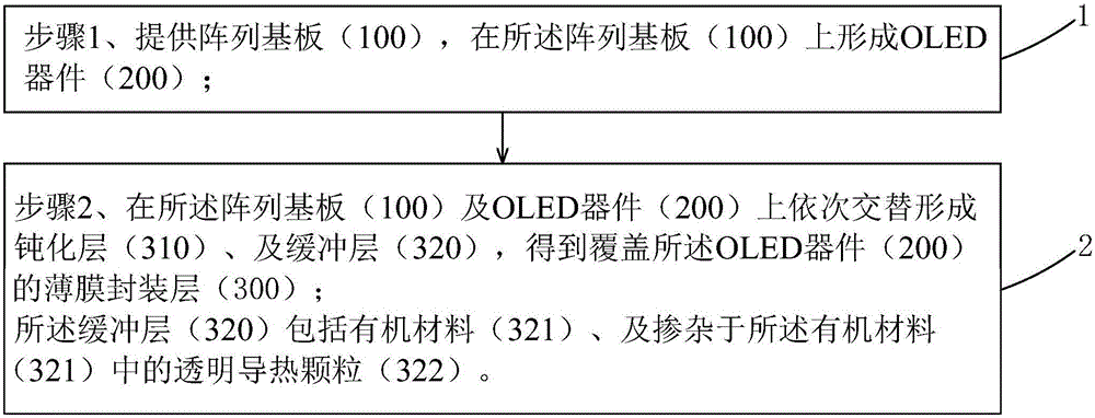
[0029] see figure 2 , the present invention provides an OLED display device, comprising an array substrate 100, an OLED device 200 disposed on the array substrate 100, and a thin film disposed on the array substrate 100 and the OLED device 200 and covering the OLED device 200 encapsulation layer 300;

[0030] The thin film encapsulation layer 300 includes a passivation layer 310 and a buffer layer 320 alternately stacked in sequence, and the number of layers of the passivation layer 310 and the buffer layer 320 is at least one layer;

[0031] The buffer layer 320 includes an organic material 321 and transparent heat-conducting particles 322 doped in the organic material 321 .

[0032] Specifically, the array substrate 100 includes a base su...


PUM


Abstract

The invention provides an OLED (organic light emitting diode) displaying device and a manufacturing method thereof. The OLED displaying device comprises an array substrate, an OLED device and thin film packaging layers, the OLED device is arranged on the array substrate, the thin film packaging layers are arranged on the array substrate and the OLED device, cover the OLED device and include passivation layers and buffering layers which are arranged alternatively in sequence. The buffering layers comprise organic materials and transparent heat-conducting particles doped in the organic materials. By means of doping the transparent heat-conducting particles in the organic materials, heat conduction efficiency of the buffering layers can be increased, heat conduction efficiency of the thin-film packaging layers can be increased further, working temperature of the OLED device can be lowered, material degradation of the OLED device is avoided from being accelerated due to temperature raising of the OLED device, and service life of the OLED displaying device is prolonged.

Description

technical field [0001] The invention relates to the field of flat panel display technology, in particular to an OLED display device and a manufacturing method thereof. Background technique [0002] Organic Light-Emitting Diode (OLED) display devices have the characteristics of self-illumination, high brightness, wide viewing angle, high contrast, flexibility, and low energy consumption. , has begun to gradually replace traditional liquid crystal display devices. At present, the application of OLED display panels has become a high-end symbol from small-sized mobile phone display screens to large-sized high-resolution flat-panel TVs. [0003] Unlike traditional liquid crystal display technology, OLED display technology does not require a backlight, and uses very thin coatings of organic materials and glass substrates that emit light when an electric current passes through them. However, because organic materials are easy to react with water vapor or oxygen, as a display devi...

Claims


Application Information

Patent Timeline
Patent Type & Authority Applications(China)
IPC IPC(8): H01L51/52H01L27/32
CPCH10K59/12H10K50/87H10K50/844H10K2102/331H10K59/1201
Inventor 杨杰余威
Owner WUHAN CHINA STAR OPTOELECTRONICS TECH CO LTD
Why Eureka
Try Eureka